For the current loop, you need to pay attention to the following basic items:
1. If you use a trace, you should make it as thick as possible
When considering the grounding connection on the PCB, the design should be as thick as possible. This is a good rule of thumb, but be aware that the minimum width of the ground wire is the effective width from this point to the end, where "end" refers to the point furthest from the power connection.
2. Ground loops should be avoided
3. If the ground plane cannot be used, a star connection strategy should be used (see Figure 6).
In this way, the ground current is independently returned to the power supply connection. In Figure 6, it is noted that not all devices have their own loops, U1 and U2 are shared loops. This can be done by following the guidelines in Articles 4 and 5 below.
4. Digital current should not flow through the analog device
When the digital device is switched, the digital current in the loop is quite large, but only instantaneous. This phenomenon is caused by the effective inductance and impedance of the ground. For the inductive part of the ground plane or ground trace, the formula is V = Ldi/dt, where V is the generated voltage, L is the inductive reactance of the ground plane or ground trace, di is the current change of the digital device, dt is duration. The influence on the ground impedance portion is calculated as V = RI, where V is the generated voltage, R is the impedance of the ground plane or ground trace, and I is the current change caused by the digital device. These voltage changes across the ground plane or ground trace of the analog device will change the relationship between the signal and ground in the signal chain (ie, the voltage to ground of the signal).
5. High speed current should not flow through low speed devices
Similar to the above, the ground return signal of the high speed circuit also causes the voltage of the ground plane to change. The calculation formula for this interference is the same as above, for the inductive reactance of the ground plane or ground trace, V = Ldi/dt; for the impedance of the ground plane or ground trace, V = RI. As with digital currents, when the ground plane or ground trace of a high-speed circuit passes through an analog device, the voltage change on the ground line changes the relationship between the signal and ground in the signal chain.
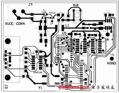
Figure 4 shows the top layer of the circuit board designed with the manual schematic as shown in Figure 3.

Figure 5 shows the bottom layer of the circuit board designed by the schematic diagram shown in Figure 3.
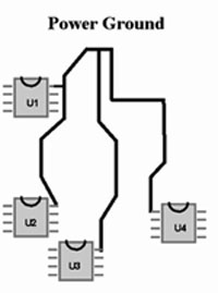
Figure 6 If the ground plane cannot be used, the “star†routing strategy can be used to handle the current loop.
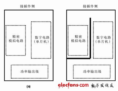
Figure 7 is separated by a ground plane that is sometimes more effective than a continuous ground plane. Figure b) The grounding strategy is better than the grounding strategy of Figure a)
6. Regardless of the technology used, the ground loop must be designed for minimum impedance and capacitive reactance
7. If the ground plane is used, separating the ground plane may improve or reduce the circuit performance, so use it with caution.
An effective method of separating the analog and digital ground planes is shown in Figure 7.
In Figure 7, the precision analog circuit is closer to the connector, but is isolated from the switching currents of the digital network and the power circuit. This is a very efficient way to separate the ground loops, and we have used this technique in the wiring of Figures 4 and 5 discussed earlier.
Lead Free Piezoelectric Elements
The Co-Al Co-doped Barium Titanate Lead-free Piezoelectric Ceramics was successfully developed by Yuhai company through repeated experiments. By Researching the influence of Co-Al Co-doping on the structure and properties of Barium Titanate-based piezoelectric ceramics, the formulation and preparation technology of Barium Titanate-based piezoelectric ceramics were optimized. Yuhai`s BaTiO3 was prepared by conventional solid-phase sintering method, with the piezoelectric constant d33 (>170pC/N), dielectric loss tgδ≤0.5% and mechanical coupling coefficient Kp≥0.34.
Barium titanate lead-free piezoelectric ceramics are important basic materials for the development of modern science and technology, which was widely used in the manufacture of ultrasonic transducers, underwater acoustic transducers, electroacoustic transducers, ceramic filters, ceramic transformers, ceramic frequency discriminators, high voltage generators, infrared detectors, surface acoustic wave devices, electro-optic devices, ignition and detonation devices, and piezoelectric gyroscope and so on.
Application: military, ocean, fishery, scientific research, mine detection, daily life and other fields.
China Patent of Yuhai company`s BaTiO3
Chinese Patent No.: ZL 2011 1 0126758.6
Name: Lead-free Barium Titanate Piezoelectric Material with Addition of Cobalt and Aluminum

|
Lead free piezo material BaTiO3 |
Lead-free Material |
||
|
Properties |
|
|
BaTiO3 |
|
Dielectric Constant |
ɛTr3 |
|
1260 |
|
Coupling factor |
KP |
|
0.34 |
|
|
K31 |
|
0.196 |
|
|
K33 |
|
0.43 |
|
|
Kt |
|
0.32 |
|
Piezoelectric coefficient |
d31 |
10-12m/v |
-60 |
|
|
d33 |
10-12m/v |
160 |
|
|
g31 |
10-3vm/n |
-5.4 |
|
|
g33 |
10-3vm/n |
14.3 |
|
Frequency coefficients |
Np |
|
3180 |
|
|
N1 |
|
2280 |
|
|
N3 |
|
|
|
|
Nt |
|
2675 |
|
Elastic compliance coefficient |
Se11 |
10-12m2/n |
8.4 |
|
Machanical quality factor |
Qm |
|
1200 |
|
Dielectric loss factor |
Tg δ |
% |
0.5 |
|
Density |
Ï |
g/cm3 |
5.6 |
|
Curie Temperature |
Tc |
°C |
115 |
|
Young's modulus |
YE11 |
<109N/m3 |
119 |
|
Poison Ratio |
|
|
0.33 |
Piezo Element,Piezo Ceramic Elements,Piezoelectric Ceramic,Pzt Tubes
Zibo Yuhai Electronic Ceramic Co., Ltd. , https://www.yhpiezo.com