After the soldering is completed, the PCB needs to be tested on its components. The traditional method is to solder it off the PCB board and test it. However, this method is not only cumbersome, low in efficiency, but also easy to damage the board and extremely impractical; another method is Manually combined with the machine for testing, but this requires the tester to have some experience, but also brings certain uncertainty to the test, so that the accuracy of the test results can not meet the reliability requirements of modern circuit boards. Therefore, this paper studies a feasible, simple, practical and high precision capacitor online test circuit. In addition, with the rapid development of EDA technology, FPGA is rapidly becoming a digital system development platform with its high integration, high reliability and flexibility, and has a very broad application prospect in various fields. This design combines the above two characteristics to design a capacitor online test circuit based on implanting Nios II embedded soft core into the FPGA as controller.
Test principle
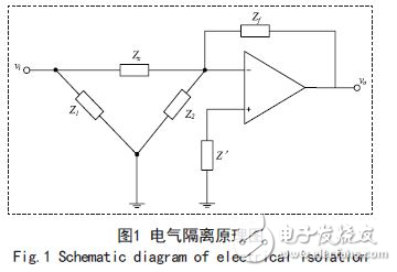
The basic idea of ​​online testing is to apply electrical isolation technology to electrically isolate the component under test from the components connected to it, and then to detect each component on the PCB. The isolation method is shown in Figure 1. Let the device under test be Zx, and the impedance of the components connected to it is equivalent to Z1 and Z2, and the other end of the device is in the same ground as the test circuit. Because the op amp is grounded to the input terminal, according to the "virtual ground" principle, the equipotential at both ends of Z2 is ground, that is, Z2 is isolated; when Vi is an ideal voltage source, the internal resistance is zero, and Z1 can be regarded as a voltage source. The output load does not affect the voltage drop across Zx, ie Z1 is also isolated. It can be seen that as long as the input is determined and the output is measured, the size of the device under test can be calculated.
Signal source circuit
Capacitance testing requires an ac signal at the input of the test circuit and requires an adjustable frequency. In this paper, the DDS dedicated chip AD9850 is used to design the AC signal source. The AD9850 has a 40-bit control word inside, 32 bits for frequency control, 5 bits for phase control, 1 bit for power sleep control, and 2 bits for select mode of operation. The 40-bit control word can be connected to the controller FPGA in parallel or serial mode. This article uses the serial load control word to save the I/O port. Figure 3 shows the serial loading timing chart of the control word.
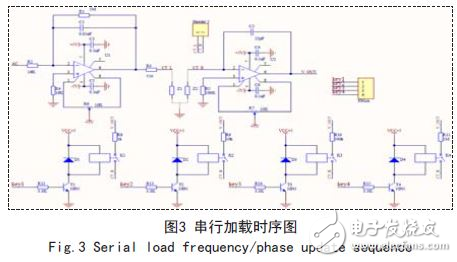
In the serial input mode, one bit of data of data bit D7 is serially input on the rising edge of W_CLK. When 40 bits are input, the output frequency and phase can be updated with one FQ_UD pulse. Figure 4 is a circuit diagram of the DDS hardware.
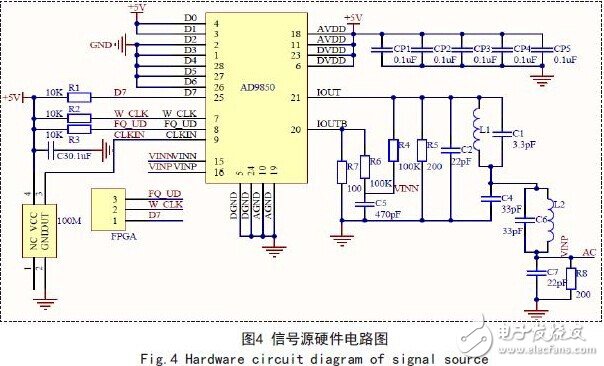
Among them, D0~D7 are eight-bit data input port, and the internal register is loaded with 40-bit control data. This article uses serial input, so only D7 bit is used to connect with FPGA; CLKIN is external reference clock input, this design adopts 100M external Clock input; W_CLK is the word input signal, the rising edge is valid; FQ_UD is the frequency update control signal, the rising edge of the clock confirms that the input data is valid; VINP and VINN are the positive and negative inputs of the internal comparator respectively; IOUT is the internal DAC output; IOUTB It is the “complementary†DAC output; AVDD and DVDD are powered by +5V. The IOUT output signal passes through the filter and acts as an excitation signal for the test circuit.
Through the comparison between the above measured values ​​and the standard values, it can be seen that the FPGA-controlled capacitor online test system designed in this paper has multi-range automatic selection, high test accuracy and convenient use. The test range is 0.01μF~3μF. After theoretical analysis and Tests have shown that the design is highly practical and reliable.
Power 12W ,output voltage 3-12V, output current Max 1A, 6 dc tips. We can meet your specific requirement of the products, like label design. The material of this product is PC+ABS. All condition of our product is 100% brand new.
Our products built with input/output overvoltage protection, input/output overcurrent protection, over temperature protection, over power protection and short circuit protection. You can send more details of this product, so that we can offer best service to you!
12W Wall Adapter, 12W Wall Power Supply,12W Power Cord In Wall, 12W Wall Power Adapter
Shenzhen Waweis Technology Co., Ltd. , https://www.laptopsasdapter.com