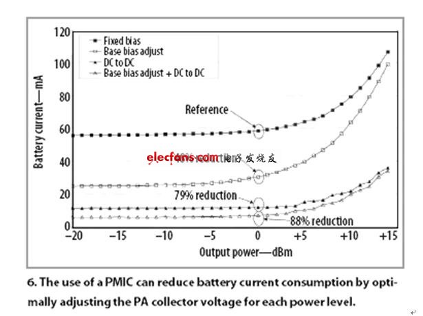
The RF6280 DC-DC converter is equivalent to a pulse width modulation (PWM) voltage mode controller that increases the Vset voltage by a factor of 2.5 [Vout = 2.5 (Vset)]. The PA collector voltage at each power stage is optimized using a DC-DC converter, and the reduction in battery power consumption is almost equal to the ratio of Vout/Vin. Use the formula Pout=?Pin for DC-DC converters, here? On behalf of efficiency, the formula Ibat = (Vout / ? Vin) Iload of the battery current (Ibat) can be derived, where Iload represents the load current. This equation shows that the battery current is the ratio of Vout/Vin, assuming a converter efficiency of 100% and a constant load across all operating voltage levels.
This article refers to the address: http://
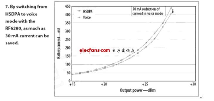
Compared to the HSDPA modulated signal, the peak-to-average power ratio of the speech modulated signal is smaller. Since the handset must operate in two modes, the PA bias must be high enough to maintain sufficient linearity to achieve system adjacent channel leakage ratio (ACLR) requirements. Once the PA bias voltage is set to meet HSDPA requirements, these same voltage levels provide additional ACLR margin in voice mode of operation. Since this extra ACLR margin is not required, ACLR performance may be sacrificed to save more battery power. In Figure 7, in the voice mode of operation, by reducing the control voltage set in the HSDPA mode of operation, 30 mA of power can be saved at the highest power level. This flexibility allows designers to trade off linearity margins, slopes, and power based on operating modes.
The heat dissipation of mobile phones is still a concern of designers. The power amplifier (PA) is the main heat generating device. The use of a DC-DC converter will operate the PA collector voltage to a minimum specified voltage and maximum output power (independent of battery voltage). The RF6285 operating at maximum output power is used as an example to illustrate how to reduce power consumption by using a DC-DC converter.
When the output power is +27-dBm, the typical power consumption of the RF6285 is 450mA. As shown by the formula Pdiss=Pin-Pout, the power consumption is a function of the input power and the output power. Since Pout is constant at +27 dBm (0.5 W), it is determined by Pin that the power consumption of the PA is. When the PA is used under full charge battery power and no power management, the value of Pin is: Pin=4.5VX0.45A=2.03W, and the power consumption is 1.53W. In the case of power management, the PA collector is set to 3.1V, so Pin=3.1VX0.45A=1.39W, and the power consumption is only 0.89W. This reduction in voltage reduces PA power consumption by approximately 42%, which means that the PA chip temperature will drop by 42 °C.
For operators and handset manufacturers, the field performance of mobile phones is critical. EVM and ACLR system requirements, as well as total radiated power (TRP) and specific absorption rate (SAR) limits, require robust performance under mismatched load conditions. In addition, post-calibration handsets may be adversely affected in terms of efficiency and power accuracy. PA load sensitivity is important for the overall performance of the transmit link. An orthogonal architecture is used in RF6281, RF6285, RF6241, RF6242, and RF6245 PA to reduce PA load sensitivity. These devices are designed with parallel path amplifiers with lead/lag separators and synthesizer networks. In use, the wireless network can create amplifier paths that are 90 degrees out of phase with each other, which requires the PA to work robustly.
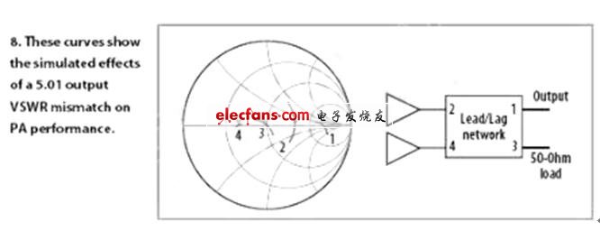
Figure 8 shows what happens when the lead/lag synthesizer network output mismatch. In this simulation, there is a 5.0:1 VSWR mismatch on the Port1 synthesizer output. The reason for using 5.0:1 VSWR is that this is the worst mismatch that can occur in a mobile environment. Ports 2 and 4 are affected by impedance conversion, which means that each PA outputs 2.0:1 VSWR. The front-end component insertion loss can isolate the antenna mismatch. Typical front-end component insertion loss is at least 3dB, which limits the worst-case VSWR of the lead/lag synthesizer output to 3.0:1 instead of 5.0:1.
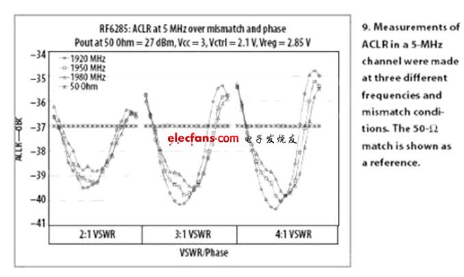
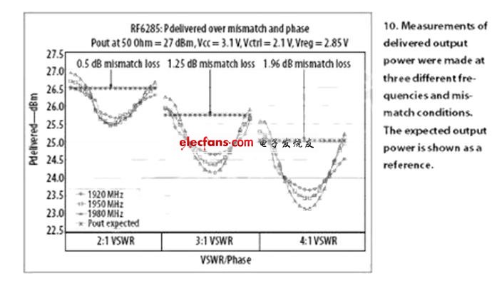
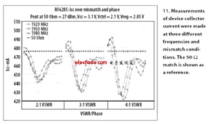
Figure 9 shows the measured relationship between the ACLR performance of the RF6285 and the VSWR, from which the advantages of the PA orthogonal architecture can be seen. For reference, in the worst case VSWR of 3.0:1, the ACLR drops by less than 2 dB, compared to 10 dB for a single-ended PA. For a worst case VSWR of 3.0:1, the power of the RF6285 drops by only 2.5 dB, compared to 3.5 dB for a single-ended PA (Figure 10). Figure 11 shows the peak collector current of RF6285 versus VSWR. In the worst case VSWR of 2.0:1, the peak collector current of RF6285 increased by only 3%, while the single-ended PA increased by as much as 20% under the same conditions.
The designers of 3G mobile phones face a lot of challenges, and it is necessary to solve those problems first, depending on the final application. Solutions like the RD6280 module offer the flexibility of multi-band applications while maintaining optimal performance at all power levels and operating modes. Conversely, highly integrated solutions such as RF6241, RF6242, and RF6245 reduce component count. Both of these solutions are designed to meet the power requirements of improved back-off power levels, while the RD6280 includes PA PMIC for more performance optimization.
Comcn Electronics Limited , https://www.comcnspeaker.com