1.1 Introduction
Human fingerprints are one of the biological features. Fingerprint recognition is the most mature biometric technology. Its uniqueness and stability have always been regarded as one of the reliable means of identity identification. In today's college life, the physical quality of college students gradually falls short of standards, and schools need to guide students to exercise. However, if manual management is very inconvenient, it is relatively simple to perform machine intelligent management. Fingerprint recognition can manage the information of each student in a unified way, which promotes the school's management of students' physical exercise.
1.2 Project Background / Motivation
The system is based on Xilinx's FPGA development platform NexysTM3 Spartan-6 as the core control device. This device has 48M bytes of external memory and a wealth of I/O devices and interfaces for this system. Through some high-precision fingerprint recognition algorithms, and then through FPGA operations, we achieve the capture, storage, processing and comparison functions of fingerprint images. SDRAM and Flash are used to store temporary data and fingerprint data information when the fingerprint program is running. At the same time, through the USB and the computer, establish a database in the computer, and realize the communication between the FPGA and the computer, complete the fingerprint identification management system.
Second, the demand analysis2.1 Functional requirements
Fingerprint information is collected using a fingerprint collector and transmitted to SDRAM storage. Fingerprints are processed and matched on the FPGA, and programs are written to allow the FPGA to communicate with the computer and build a database on the computer so that data management can be done using the computer's database.
2.2 Performance requirements
A fingerprint recognition system that is accurate, fast, and practical. At the same time, a good FPGA and computer communication function is realized.
2.3 System Highlights
The main difficulty of this system lies in the algorithm of fingerprint recognition and the driver that XILINX needs to write when communicating with PC.
Third, the program design3.1 System function realization principle
The system uses Xilinx Spartan 6 series FPGA as the core control chip, and the fingerprint is transmitted to the memory SDRAM storage through the FPC1011F sensor. The fingerprint processing program running on Spartan processes the fingerprint information to obtain feature points, and stores them in the SDRAM or matches the fingerprint information in the SDRAM. Finally, communicate with the computer via USB, using the student database in the computer.
The system block diagram is as shown:

3.2 Hardware platform selection and resource configuration
3.2.1 Fingerprint sensor FPC1011F
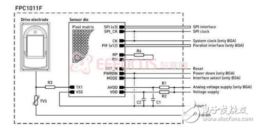
The FPC1011F is a capacitive face-mounted fingerprint sensor successfully launched by Fingerprint Cards of Sweden. The sensor uses a number of patents, such as independent wafer body signal amplification, protective film on the sensor surface. The internal A/D conversion, high-speed SPI interface, 8PIN soft cable can easily access a variety of systems.
The FPC1011F fingerprint sensor has the following features:
(1) The FPC1011F chip is produced in Sweden and uses a unique reflective measurement method. The antistatic can reach 15kV or more and wear 1 million times. It has been recognized by the domestic financial community as a designated part of the bank.
(2) Using the professional fingerprint identification chip PS1802DSP and optimized fingerprint algorithm, the fingerprint imaging effect is good.
(3) The processing speed is fast, the peak value can reach 480 MIPS, and in the 1:1 000 mode, the time is less than 1 s.
(4) The power consumption is lower than that of similar products. The normal working frequency is 120 MHz, only 120 mW.
(5) The module volume is 35 mm & TImes; 26 mm & TImes; 1 mm, which is convenient for the development of various fingerprint products.
(6) Automatic adjustment function for wet and dry fingers.
The FPC1011F fingerprint sensor contains a small capacitive plate. The sensor uses a high-sensitivity pixel amplifier that allows each pixel to be detected even by the very weak signal FPC1011F, thereby improving image quality. Alternating commands are used and arranged in parallel with the sensor plates. The alternating plates are in the form of two capacitive plates, and the valleys and ridges of the fingerprints become the dielectric between the plates. A constant dielectric sensor between the two detects changes to generate a fingerprint image.
3.2.2 SPI communication interface
The SPI interface is mainly used in EEPROM, FLASH, real-time clock, AD converter, and between digital signal processor and digital signal decoder. SPI is a high-speed, full-duplex, synchronous communication bus that occupies only four wires on the pins of the chip, saving the pins of the chip and saving space for the layout of the PCB. Because of this simple and easy to use feature, more and more chips are now integrating this communication protocol.
The SPI bus system is a synchronous serial peripheral interface that allows the MCU to communicate serially with various peripherals to exchange information. Peripheral settings FLASHRAM, network controller, LCD display driver, A/D converter and MCU. The SPI bus system can directly interface with a variety of standard peripheral devices produced by various manufacturers. This interface generally uses 4 lines: serial clock line (SCK), master input/slave output data line MISO, master output/slave input. The data line MOSI and the active low slave select line SS (some SPI interface chips have an interrupt signal line INT, and some SPI interface chips have no master output/slave input data line MOSI).
The communication principle of SPI is very simple. It works in master-slave mode. This mode usually has one master device and one or more slave devices. It requires at least 4 wires. In fact, 3 can also be used (for one-way transmission, That is half-duplex mode). Also common to all SPI-based devices, they are SDI (data input), SDO (data output), SCK (clock), CS (chip select).
SDO – Master device data output, slave device data input.
SDI – Master device data input, slave device data output.
SCLK – Clock signal, generated by the master device.
CS – Slave enable signal, controlled by the master.
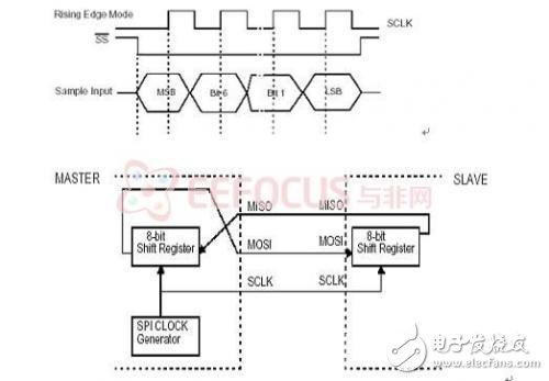
Figure 3.3 SPI interface signal
Where CS is the control chip is selected, that is to say, only when the chip select signal is a predetermined enable signal (high potential or low potential), the operation of the chip is effective. This makes it possible to connect multiple SPI devices on the same bus. Next, I will be responsible for the 3 lines of communication. Communication is done through data exchange. Here we must first know that SPI is a serial communication protocol, that is to say, the data is transmitted one bit at a time. This is the reason for the existence of the SCK clock line. The clock is supplied by SCK, and SDI and SDO complete the data transmission based on this pulse. The data is output through the SDO line, the data changes on the rising or falling edge of the clock, and is read on the next falling or rising edge. Complete a data transfer and use the same principle for input. Thus, the transmission of 8-bit data can be completed at least 8 times of the change of the clock signal (the upper edge and the lower edge are once).
It should be noted that the SCK signal line is only controlled by the master device, and the slave device cannot control the signal line. Similarly, in an SPI-based device, there is at least one master device. The characteristics of this transmission: This transmission method has an advantage. Unlike ordinary serial communication, ordinary serial communication continuously transmits at least 8 bits of data at a time, while SPI allows data to be transmitted one bit at a time, even allowing pauses because The SCK clock line is controlled by the master device. When there is no clock transition, the slave device does not collect or transmit data. That is to say, the master device can control the communication by controlling the SCK clock line. SPI is also a data exchange protocol: because the data input and output lines of the SPI are independent, it allows simultaneous input and output of data. Different SPI devices are implemented differently, mainly because of different data change and acquisition time. There are different definitions on the edge or lower edge of the clock signal. For details, please refer to the related device documentation.
In point-to-point communication, the SPI interface does not require addressing operations and is full-duplex communication, which is simple and efficient. In a system with multiple slave devices, each slave device requires a separate enable signal, and the hardware is slightly more complicated.
The SPI interface is actually two simple shift registers in the internal hardware. The transmitted data is 8 bits. It is transmitted bit by bit under the slave enable signal and shift pulse generated by the master device. The high bit is in the front and the low bit is in the back. . As shown in Figure 3.4, the data changes on the falling edge of SCLK while one bit of data is stored in the shift register.
The FPC1011F port is mainly composed of 4 pins: SPI_CK, SPI_DO, SPI_DI, /SS, SPI_CK is the common clock of the entire SPI bus, SPI_DO, SPI_DI as the master, the input and output flags of the slave, SPI_DO is the output of the master, the slave The input, SPI_DI is the input of the master, the output of the slave. /SS is the slave's flag pin, in the two SPI bus devices that communicate with each other, the /SS pin's low level is the slave, and the opposite /SS pin's level is the master. In an SPI communication system, there must be a host. The SPI bus can be configured as a single master single slave, single master multiple slave, and mutual master.
The SPI chip select can be expanded to select 16 peripherals.
Disadvantages of the SPI interface: There is no specified flow control, no response mechanism to confirm whether data is received.
3.2.3 SDRAM
SDRAM: Synchronous dynamic random access memory, synchronous dynamic random access memory, synchronization means that the memory needs to synchronize clocks, the internal command transmission and data transmission are based on it; dynamic means that the storage array needs constant refresh to ensure data is not lost. Random refers to the fact that data is not stored in a linear order, but a freely specified address for reading and writing data.
3.2.4 FIFO module
The main function of this module is to cache the fingerprint data that has been received to avoid the loss of fingerprint data. Therefore, the SPI working frequency of this system is 16MByte, and the UART serial port operating frequency is 38MByte. So you need to set the FIFO to make the SPI and UART work together.
3.2.5 UART module
The main function of this module is to communicate with the computer and display the received data through the computer database.
3.3 system software architecture
3.3.1 Fingerprint Acquisition Procedure
Initialize the SPI interface module
Reset FPC1011 fingerprint sensor
Initialize sensor
Send start sensor command rd_sensor: 0x11
Read sensor command
Command rd_sensor (11 H)
Mode serial
Input parameter 1 virtual byte
Data delay (363 ± 2) tCLK
Return byte 0
Data latency refers to the delay of the instruction until the data in the FIFO is valid. The instruction is used to read all or part of the sensor.
This instruction is only used to turn on the sensing sequence, and the instruction itself does not return any data. The first set of data for the sensor sequence enters the FIFO after approximately 363 clock cycles. Thereafter, every 8 clock cycles, a new byte is written to the FIFO until the area defined by the XSENSE, YSENSE, XSHIFT, and YSHIFT registers is read.
If the FIFO load data is full, we will let the sensor pause until the data is read from the FIFO to prevent overflow. All analysis modules are active during the timeout and the ASIC will generate current during a normal sensing operation.
After the instruction is entered, SPI_DI will remain low as an input in case the next byte is mistaken for a new instruction.
If SPI_CS_N is set high, the read program will stop. In order to continue reading afterwards, we need to use the rd_spidata instruction.
5) Repeatedly send the read data status register command rd_spistat: 0x21 until the fingerprint data is ready.
Command rd_spistat (21 H)
Mode serial
Input parameter 1 virtual byte
Data delay 0
Return byte 1
The SPI Status Register holds the SPI interface status information. When the rd_spistat command is received, the contents of the SPI_STAT register will be returned. If the sensor read command is being executed, using this command will not interrupt the read command.
6) Send read data command rd_spidata: 0x20 Read fingerprint data and store it in SDRAM.
Read SPI data command
Command rd_spidata (20 H)
Mode serial
Input parameter 1 virtual byte
Data delay 0
Return byte n
After sending the read SPI data command rd_spidata, the fingerprint pixel data will be returned. As long as SPI_CS_N and SPI_DI remain low, the data will continue to return.
3.3.2 Software implementation of fingerprint data storage
Since the fingerprint image collected by this design is too large, and the processed image information is generated multiple times during the fingerprint image processing, we use a large-capacity SDRAM as a storage medium.
By calling EDK's own SDRAM IP core, we can easily control the SDRAM read and write operations.
SDRAM write data function:
Void XDdr_mWriteReg(Xuint32 BaseAddress, unsigned RegOffset, Xuint32 Data)
The meaning of the parameters:
BaseAddress: write data at the base address of the SDRAM
RegOffset: address offset, data is written in the SDRAM (BaseAddress+ RegOffset) position
Data: Data to be written in SDRAM
SDRAM read data function:
Void XDdr_mReadReg(Xuint32 BaseAddress, unsigned RegOffset)
The meaning of the parameters:
BaseAddress: the base address of the data read from the SDRAM
RegOffset: address offset, read data in the (BaseAddress+ RegOffset) position of the SDRAM
3.3.3 Software implementation of fingerprint image preprocessing
Fingerprint image preprocessing can be divided into several steps such as image segmentation, enhancement, binarization and refinement, but the preprocessing steps are not the same according to the specific situation. Image segmentation refers to separating fingerprint images from the background, reducing the time for subsequent processing and improving the reliability of feature extraction. There are also some literatures that will binarize the fingerprint image, that is, the fingerprint ridge (the ridge refers to the black line on the fingerprint of the finger skin bulge on the fingerprint collector; the valley refers to the blank portion between the ridges) Extracting from the fingerprint image is also classified as an image segmentation part. The purpose of image enhancement is to highlight the fingerprint line structure and suppress noise interference in the line and background; binarization is to change the fingerprint image into a binary image; the refinement is the fingerprint image that has been processed in the previous two steps. The width of the ridge of the fingerprint is minimized, the burrs on the original line are removed, the lines are sharper, and the false intersections and breakpoints generated by the burrs are minimized.
3.3.4 Feature point extraction of fingerprint images
The commonly used fingerprint feature description method is based on the texture structure feature. Fingerprint features can be divided into global features, local features, and subtle features. The global features include: (i) basic grain pattern: the basic grain pattern is usually divided into a left-hand type (letfloop), a right-hand type (rightloop), a bucket type (whorl), an arch type (acrh), and an arched type (etntedacrh). As shown in Figure 4.6. (ii) Pattern area (PattemAera): The pattern area is an area on the fingerprint image that contains the overall features. The pattern area can distinguish which type of fingerprint belongs to. (iii) Core Point: The core point is located at the asymptotic center of the fingerprint pattern, which is often used as a reference point for reading fingerprints and comparing fingerprints. (iv) Delta point (Detla): The triangle point is the center point of the triangle grain area in the fingerprint image. The three fingerprint lines closest to the point form an approximate equilateral triangle. The triangle point provides the starting of the fingerprint pattern count and tracking. position. Core points and triangle points are collectively referred to as singular points. (v) Ridge Cuont: As a global feature, the number of lines generally refers to the number of fingerprint lines in the pattern area. Some algorithms use the number of lines between two points as fingerprint features, such as the number of lines between two nodes.

(1) left-hand type (2) right-hand type (3) bucket type (4) arch type (5) pointed arch type
Figure 4.6 Basic pattern
Local features include: (i) Ending: A stripe road ends here. (ii) BiofcraTIno: A striped road is divided into two or more striped roads here. (iii) Ridge Divegrneee: Two parallel lines are separated here. (iv) Dot or Island: A particularly short grain that is so little. (v) ShortRidge: A pattern that is shorter but does not become a point. (vi) Enclosuer: A stripe road is divided into two and then one is formed immediately. A small loop thus formed is called a loop point. (vii) Bridge: Two parallel lines are lapped here. (viii) Curvuter: The speed at which the direction of the grain changes. As shown in Figure 4.7.
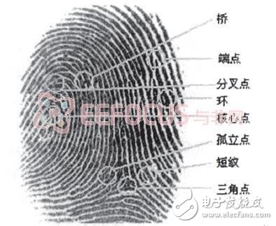
Figure 4.7 Basic pattern
In addition, in addition to local features, high-quality fingerprint images acquired from high-resolution sensors can also extract features that are more subtle than local features: pores. The extraction of pore characteristics generally requires a sensor resolution of 1000 dpi and requires high finger skin quality. However, the resolution of the fingerprint sensor is generally around 500 dpi, and it is often difficult to accurately extract the pore characteristics in the captured image due to environmental and skin conditions, so the pore characteristics are generally not used in the actual system.
3.3.5 Matching of fingerprint images
After the pre-processing and feature extraction of the fingerprint image, a large amount of redundant information has been eliminated, and the real feature data representing the fingerprint feature itself is obtained. Fingerprint matching is to compare the similarity of the feature data of two fingerprint images.
3.3.6 FPGA and computer communication
In order to realize that the fingerprint can communicate with the database, it is necessary to use the communication of the completed PC.
letter of agreement
This part mainly completes the fingerprint matching feature information and returns the result. The returned result is displayed on the LCD.
This process requires defining a flag definition for the frame. It takes a long time to consider.
Different development platforms are different in their difficulty in applying to different fields. Therefore, fingerprint recognition and matching are programmed using MATLAB, while COM+ has the advantage of cross-platform calling and is easy to operate. So COM+ component technology is used as part of the database interface. The database interface part uses the ACESS database.
The system is expected to implement access to fingerprint feature information, update user information and other related operations.
4. System software process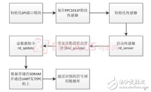
(Finish)
200*300mm Anti-Blue Light Film
The Imported Anti-Blue Light For ipad is made of high-quality imported TPU material. It is precisely cut by the Screen Protector Cutting Machine. Protect your device screen from scratches and cracks. The flexible TPU Screen Protector can completely cover the iPad screen, providing the maximum protection for the iPad.
Advanced blue light blocking technology can protect your eyes, can effectively filter blue light, prevent glare, reduce eye fatigue, and help you fall asleep better.
Super clear and transparent, will not reduce the screen brightness, maintain the original screen brightness, and reduce eye fatigue.
The Protective Film adopts an oleophobic and waterproof coating, which can ensure anti-fingerprint, waterproof, dustproof and no air bubbles. Moreover, it is sensitive to touch, bringing natural touch, fast response and flawless precise touch.
If you want to know more about Imported Anti-Blue Light For ipad products, please click product details to view the parameters, models, pictures, prices and other information about Imported Anti-Blue Light For ipad products.
Whether you are a group or an individual, we will try our best to provide you with accurate and comprehensive information about Imported Anti-Blue Light For ipad!
Imported Anti-Blue Light Protective Film, Imported Anti-Blue Screen Protective Film, Imported Anti-Blue Screen Protector, Imported Anti-Blue Light Screen Protector
Shenzhen Jianjiantong Technology Co., Ltd. , https://www.jjttpucuttingplotter.com