Ethernet is the most widely used networking technology. It is widely used in enterprises and schools in the fields of high reliability, large amount of media information, easy to expand and update. According to the IEEE802.3 Ethernet standard specification, the length of each coaxial cable of Ethernet shall not exceed 500m. After interconnection through repeaters, the maximum distance of the network shall not exceed 2.8km. In this case, the use of laser wireless communication technology, beyond the geographical limitations of Ethernet, to meet the needs of data communication, has a strong application value.
Modulation drive circuit design
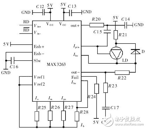
Figure 6 is a modulation drive circuit diagram mainly composed of MAXIM's 155MHz MAX3263 chip and a laser LD with a monitor diode inside. The MAX3263's internal main bias supply provides temperature-compensated bias and reference voltage outputs, Vref1 and Vref2, to program internal high-speed modulation drive circuits, lasers, and monitor diodes through resistors R25, R26, R27, and R28. The output current of the MAX3263 is controlled by an internal mirrored current source. These mirrored current sources have a 2Vbe junction temperature drift. When the reference voltage is set at 2Vbe, the junction temperature drift can be cancelled. Resistor R28 is selected to adjust the laser quiescent bias current Ibo such that Ibo is slightly less than the threshold current of the laser so that the output of the laser has a good extinction ratio. The monitoring diode inside the LD converts the light intensity change into a current Ipin, and internally generates a feedback current Ibs. By the formula Ibo=40(Ib+Ibs), the light intensity change of the laser is converted into a part of the bias current, and the feedback acts on The laser ensures a stable output of optical power. The input differential PECL signal RD is modulated by a modulator consisting of an internal high-speed input buffer and a common-emitter differential output. The magnitude of the modulation current is determined by the current Im determined by R26. Select the size of R26 to have the laser have the proper modulation current, output enough optical power, and have a good extinction ratio. At the same time, the voltage at the OUT+ and OUT- terminals should be above 2.2V to prevent the laser from saturating.

Figure 6 modulation drive circuit
Receive demodulation circuit design
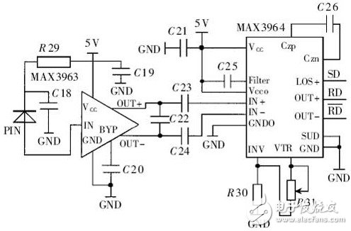
Figure 7 is a diagram of the receive demodulation circuit, which is composed of the MAX3963 and MAX3964 with the necessary peripheral components. The 155MHz low-noise chip MAX3963 consists of a preamplifier that contains a transimpedance preamplifier and an inverting amplifier with an emitter-following output. It integrates a 22kΩ transimpedance to convert the weak photocurrent of the PIN reception into Differential output voltage. The 266MHz MAX3964 forms a post-amplification conditioning circuit. There is a serial power detector consisting of four limiting amplifiers, each of which has a full-wave logarithmic detector to detect the power of the input signal. The four test results are added together at the Filter end and filtered by capacitor C25. Resistors R30, R31, the internal 1.2V reference supply, and the matte comparator together form a threshold setting and noise suppression. Take R30=100kΩ, R31 can be adjusted with a potentiometer of 100kΩ, then the VTR will vary from 1.2 to 2.4V. When the input signal amplitude is greater than VTR, it outputs a stable PECL level signal; when the input signal amplitude is less than VTR, the data output terminal OUT+ outputs a high level, OUT-outputs a low level, and all limiting amplifiers reject the input. The signal, and the post amplifier outputs a no-light alarm PECL signal LOS+.

Figure 7 accepting the demodulation circuit
Since the main chips in FIGS. 6 and 7 are both above 155 MHz, the two circuits constitute a transceiver circuit for careful parameter selection and PCB design, which can be applied to high-speed optical communication applications. 5 System testing Based on the various parts of the design, they were connected and the experiment of indoor Ethernet laser wireless communication was successfully carried out without optical antenna. The system is being refined and is ready to be applied to optical networks.
American Wall Switch And Socket
Wenzhou Niuniu Electric Co., Ltd. , https://www.anmuxisocket.com