Abstract: For the video data compressed by MPEG4 format, the controller design using NAND FLASH as the storage medium and FPGA as the storage array is given, and DSF is used as the core unit of data processing to complete the system design method of large-capacity video data storage. At the same time, solutions are proposed for key problems such as detection and processing of bad blocks.
Keywords: FPGA; DSP FLASH; large capacity; storage
0 Introduction The development of science and technology, especially the development of aviation, aerospace and navigation technology, the video data of scientific research equipment and the monitoring video of equipment operation, urgently need an image with large capacity, fast speed and reliable storage performance. Storage device. The traditional storage medium is mainly based on the early tape drive and the subsequent disk. Since the tape drive has low storage density and the storage content is not easy to find, it has already withdrawn from the historical stage. The disk is vulnerable to data loss after being strongly shaken, which seriously restricts its application in the fields of aviation, aerospace and navigation. Compared with traditional hard disks, NADN FLASH as an emerging semiconductor memory device has high storage density, high reliability, small size, light weight, low power consumption, long life, no noise, anti-vibration, and can adapt to harsh mechanics. And the temperature environment and other advantages. It can be seen that the research on mass storage system based on NADN FLASH has more important significance.
1 System Overview This system uses ADI's high-performance DSP chip BF533 as the core, uses the parallel peripheral interface (PPI) to receive the video data and control commands of the central control board, and transmits the processing result and the video data stored in the medium to Center control board; Sumsung's NAND FLASH chip K9WBG08U1M is used as the storage medium; Altera's FPGA chip EP2C35 is used to realize the timing control of FLASH. According to actual needs, the system uses 100 K9WBG08U1M chips, the storage depth can reach 400GB, and its secure storage rate can reach 5MB/s. The video data of the system is managed in the form of a file, that is, each video file has a file entry containing information such as a file name, a file address, and a file size. This entry is stored in the FLASH file list. When storing, downloading, cutting, deleting, etc., it is necessary to read the file list into the SDRAM of the DSP to determine the address of the target file for subsequent processing.
2 system hardware design
2.1 Chip selection K9WBG08U1M chip is addressed by multi-cycle input of 8-bit multiplexed I/O bus, which is divided into 5 cycles. The first 2 cycles input the page address (column address) of A0~A11, after 3 The page address (row address) of A12 to A30 is input in one cycle. Its single-chip storage capacity is (4G+128M)B, which is composed of two K9KAG08U0M chips, and the K9KAG08U0M chip is divided into 8 192 blocks, each with 64 pages and each page (4 K+128)B. The chip is programmed and read in page units with a typical programming time of 200μs, a maximum programming time of 700μs, a minimum write cycle of 25 ns, and a minimum serial read cycle of 50 ns; erasing in blocks, typically The erase time is 1.5 ms. There is a page register inside, in the program and read operation, first cache a page of data to be written or read into the page register, then write the programming command start page programming or send a read enable signal to start serial read. From this, the fastest write rate of FLASH can be calculated to be 4 096 B/(200μs+4 096×25 ns)≈13 Mb/s, and the safe write rate is 4 096 B/(700μs+4 096×25 nS). ≈ 5 Mb/s. Considering the safe writing of data, we chose a maximum programming time of 700μs, which is a safe write rate of 5MB/s.
2.2 System hardware structure block diagram The system acts as a subsystem of the network video storage system, and communicates with the central control board through the half-duplex interface PPI of the DSP. First, the received data is cached in the SDRAM, and then the buffered data is analyzed, the command type is discriminated, and the operation corresponding to the command is performed, and the real-time status information is returned to the central control board through the low-speed channel of the UART. Its hardware structure block diagram is shown in Figure 1.
This article refers to the address: http://
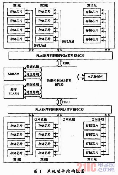
The FPGA is connected to the DSP system bus as an asynchronous peripheral of the DSP. The DSP sends data to the FPGA and reads the data in the FPGA internal RAM through the memory DMA. Considering the limitation of the number of I/O pins and the pin driving capability of the FPGA itself, the system uses two FPGAs to drive 100 FLASH. The FLASH array is divided into 25 groups, each group of 4 FLASHs, sharing a set of data/address bus. And the control bus, each piece of FLASH is selected by the chip select signal.
The video data received by the DSP's PPI interface is compressed by the MPEG-4 format, and its maximum bit flow rate is 4 Mb/s. The PPI's bus clock frequency can be up to 133 MHz, which means that the data transmission rate can be up to 133 M × 16 b / s, so the video data of 4 Mb / s can fully meet the requirements. After the video data arrives at the memory board, the FPGA is responsible for writing to the memory. The write rate of the memory chip K9WBG08U1M is 5MB/s, and the video data rate of each channel is 4Mb/s=0.5MB/s, so the memory chip K9WBG08U1M can also be stored. Rate requirements.
2.3 FLASH driver design This system uses FPGA to provide bus drive and decoding logic for FLASH. Take one FPGA as an example. The specific implementation diagram is shown in Figure 2.
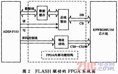
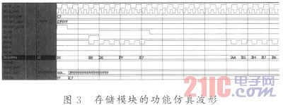
Two dual-port RAMs are built inside the FPGA, one for storage operations and one for download operations. When performing a storage operation, the FPGA first receives the data (including the address information) sent by the DSP and stores it in the dual-port RAM. This process uses the MDMA method. After the data is received, the DSP sends a start signal to the FPGA. At this time, the FPGA starts to generate the FLASH control sequence to write the data stored in the dual-port RAM to the FLASH, and simultaneously generates a corresponding chip select signal according to the address information to select a certain piece. FLASH chip. During the programming process, as long as the current page programming is completed before the end of the next MDMA, a pulse can be generated to inform the DSP to prepare for the next page write operation, which allows MDMA and programming to be performed simultaneously, thereby increasing the write rate; When the download operation is performed, the data in the FLASH is first buffered into the dual port RAM, and then the DSP is notified to perform the MDAM operation. Figure 3 shows the functional simulation waveforms for the memory operation. It can be seen from the figure that the write timing of FLASH is fully satisfied, and it is verified that the storage effect achieved by this module is very good.
3 system software design After the system power-on reset is loaded, the program enters the loop waiting state after the register initialization is completed, ready to receive the command sent by the center control. After receiving the command through the PPI, the command is analyzed to determine what operations the central control board needs to perform, such as video file storage, download, cut, copy, or delete. The file storage flow chart is shown in Figure 4.
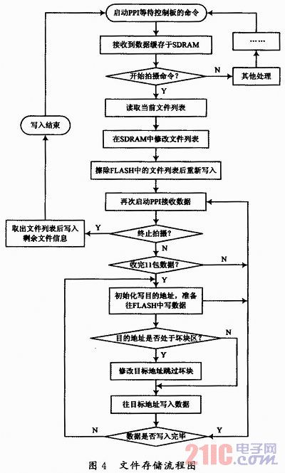
After the host computer sends a start command to the central control board through the network, the central control board first sends a start shooting command and takes video parameters to the front end video compression system, establishes a TCP link, and then sends a start command to the storage board. After receiving the command sent by the central control subsystem, the storage board first reads the file list into the SDRAM of the DSP, and the DSP retrieves the number of files and the storage address of the last file, and adds a new file entry to the SDRAM. The current file list, then erase the list of files previously stored in the FLASH and rewrite the modified file list. According to the requirements of system compression, if the code stream speed of the front-end compression is 2 Mb/s, in order to make the DSP process the data centrally, we plan to transfer the data every 4 s between the central control board and the memory board. Since the data length after each compression is not a fixed number, it can only be transmitted according to the maximum data length, that is, 1 MB per transfer. Due to the limitation of the PPI interface register bit width, the data length of each transmission cannot exceed (128K-1)B. We set the transmission length to 100 KB each time. The data received by the financial DSP through the PPI needs to pass 11 times to receive. The central control subsystem places the valid data length as a parameter at the end of the data. The memory board processes the data buffered into the SDRAM according to this parameter, and the remaining invalid data is discarded.
4 Detection of bad blocks Due to the manufacturing process and other reasons, NAND FLASH will have randomly distributed bad blocks at the factory, and FLASH will also cause bad blocks during use. If you operate on bad blocks, it will cause data loss and affect the integrity of the data. In addition, when detecting the program and erase end flags, the state of the FLASH I/O return is unstable, which causes the program to enter an infinite wait state, which greatly affects the performance of the entire system. Therefore, it is necessary to perform bad block detection and processing on the FLASH.
There are two ways to detect bad blocks: one method is to use the bad block information given by the manufacturer when the chip is shipped from the factory, which is marked by the manufacturer in the first byte of the spare block of the first page and the second page of the bad block, that is, the page. The inner address (column address) is in the byte of 4 096. If both bytes are 0xFF, it indicates that the current block is not a bad block, otherwise it is a bad block. Another method is to erase the current block first and then read the data of the current block. If the read data is not all 0xFF, it indicates that the block is a bad block (considering that the spare space is not used).
Since the bad block and the effective block are independent of each other and do not affect each other, it is only necessary to skip the bad block when operating the FLASH. Considering that the video data of the system is stored in the form of a file, that is, the DSP needs to know the storage address of the file accurately before the read and write operation, including the start address and the end address of the file, so the detected bad block table must be stored. In the memory of the DSP. If the bad block list is stored in NAND FLASH, there will be a problem: how to store the bad block list itself in the bad block area, if it is special processing, it will affect the consistency of the program. In addition, the bad block list must be read from the NAND FLASH before each search, so that the program will enter several interrupts, thus affecting the flow of the entire program. Considering that the program burns FLASH with 16 Mb, and the DSP program does not exceed 20 KB, the bad block list can be placed in the program to write FLASH, that is to say, the program burns FLASH to store both the program and the bad block list. In this way, the DSP can directly access the bad block list.
5 Conclusion In the whole system test process, this part works normally, access to NAND FLASH can skip bad blocks, to ensure the correctness and integrity of the data. In addition, how to use the pipeline method to increase the storage rate is the focus of future research.
AC (Alternating Current) Power cord is to transmit high voltage. It is used to drive machinery or home appliances. Since AC Power Cord is output of high voltage electric power, there is a risk of electric shock injury, therefore, All the AC power cord must comply with safety standard to produce. DC (direct Current) power cord is used to the applicance with lower voltage mostly, so safety requirement is less stringent.
Power Cable, battery cable, DC power cable, AC power cable, power cord
ETOP WIREHARNESS LIMITED , https://www.wireharnessetop.com