Today's cloud data centers need to process about 5 trillion gigabytes of data per year, and with millions of new users joining the cloud-connected army and the launch of new Internet of Things (IoT) facilities, this number There will also be a growth in geometric progression over the next few years. This requires cloud data centers to continue to reduce costs and have the potential for ultra-large-scale growth. MACOM's End Face Etching Technology (EFT) is able to drive the disruptive development of optical interconnects in cloud data centers, enabling cloud data centers to achieve double breakthroughs in cost and mass production.

In order to meet this rapidly growing bandwidth demand, each cloud data center is rapidly transitioning to 100G optical interconnects and preparing for the gradual move to 200G, 400G or higher, while reducing the average per averaging through scalable policies. cost. However, as of now, 100G optical interconnects need to invest heavily in mainstream commercial applications in cloud data centers, and the high cost is prohibitive. But the experience of telecom service providers has proven that investing in 100G technology is a debating deployment for decades. In view of this, cloud data center operators will perform network upgrades every three to five years to account for the existing Infrastructure 1/5's cost structure gradually increases bandwidth capacity.
Mature technology
MACOM has advanced end face etching (EFT) technology and commercial-scale manufacturing capabilities. This competitive advantage helps MACOM to grasp the development opportunities of 100G technology in the cloud data center field, and create a brilliant performance like the previous PON market. The cost reduction brings new breakthroughs. PON is currently the world's largest market for DFB lasers and is extremely sensitive to capacity and cost.
With the use of EFT technology and the use of 4-inch InP wafers, MACOM has delivered more than 200 million lasers of less than 10G to the PON market. According to MACOM, MACOM's market share in 2016 has exceeded 70%. In the cloud data center field, with MACOM's existing manufacturing capabilities, MACOM is estimated to be able to meet the production capacity of 10 million units, thus extending the significant advantages in the PON market to a huge market with higher cost per bit.
Manufacturing Efficiency EFT takes advantage of the cost structure of wafer-level manufacturing to overcome the inherent limitations of traditional cut-end technology (CFT), creating cost and productivity advantages, and significantly reducing the manufacturing cost of lasers for optical modules.
CFT technology lasers use mechanical cutting. This lack of precision can cause a large number of anomalies that affect light emission, thereby increasing the risk of laser defects. In contrast, EFT's high-precision chemical etching minimizes the risk of defects and maximizes throughput. This also reduces the manufacturing cost of the laser and lays the foundation for a more cost-effective final solution. Electron beam lithography or holographic definition is an important part of MACOM's integration of EFT technology into distributed feedback lasers, which produces high-precision gratings for ideal wavelength control.
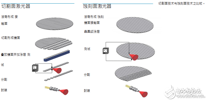
Competing products using CFT must cut the wafer into crystal strips to form the end faces of the laser cavity, while MACOM's EFT method enables wafer-level processing to complete laser formation based on the entire wafer. Clarde testing of CFT lasers is costly and can only be performed at room temperature, while wafer-level EFT lasers can be tested at full temperature per laser, are extremely efficient, and completely avoid any downstream lasers. Package.
MACOM's 25G laser portfolio for 100G cloud data center applications combines the inherent advantages of EFT. MACOM's 25G laser portfolio leverages our proprietary wafer-level InP manufacturing advantages, drawing on our valuable experience in the highly competitive cost-sensitive PON market, reflecting the cost and capacity advantages of existing mainstream laser suppliers. Consolidate our leadership position in the industry and contribute to supporting the explosive growth of cloud data centers.
From laser to L-PIC
Based on the success of EFT lasers, MACOM quickly developed a deeper development of EFT, using EFT to seamlessly integrate optical devices (including lasers, modulators and multiplexers) onto a single silicon chip, and launched the industry for 100G applications. The first silicon photonic integrated circuit (PIC) with integrated laser (L-PICTM). MACOM solves the challenge of integrating laser and silicon photonic integrated circuits with high output and high coupling efficiency, making it possible to realize high-speed, high-density optical interconnection in cloud data centers using silicon photonic integrated circuits.

The inherent characteristics of CFT lasers make them susceptible to defects affecting the accuracy of light emission. Therefore, silicon photonic integrated circuits using CFT lasers require a cumbersome assembly process, and the laser must be actively aligned to the silicon chip: first, the laser is powered up, the optical coupling is improved by physical operation, and then locked in place. This process is both time consuming and costly, and to date, the optical coupling efficiency achieved by CFT is only 50%.
With MACOM's EFT technology, both the laser surface and the silicon chip are defined by high-precision lithography, and the EFT laser is mounted on the chip in a standard flip-chip process through a proprietary self-aligned (SAEFTTM) process. Both edge emitting and surface emitting lasers are supported. This end-to-end lithography process ensures that the laser output and input waveguide positioning are precisely known. This eliminates the costly and cumbersome mechanical alignment process required for CFT while ensuring up to 80% optical coupling efficiency and unmatched device uniformity.
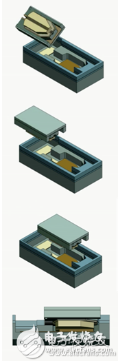
Self-aligned etched surface technology process
Compared to CFT lasers, EFT lasers have other advantages that affect the size and cost of silicon photonic integrated circuits. CFT lasers need to be hermetically sealed to avoid performance degradation caused by the laser operating in a humid environment due to mechanical cutting and subsequent strip-level coating of the laser face. With the EFT laser, the laser surface can be precisely lithographically defined to provide continuous protection coverage for the waveguide surface and the laser surface, eliminating the need for a hermetic package.
Because it does not require a hermetic package, EFT lasers can significantly reduce the size and cost of the final component and allow the silicon photonic integrated circuit to be directly on the module board, increasing the interconnect density that silicon photons can achieve.
Unparalleled innovation MACOM leverages solid leadership in EFT and protected intellectual property, combined with proven flip-chip assembly processes and large-scale manufacturing capabilities, breaking the cost of mainstream implementation of silicon photonic integrated circuits in cloud data centers barrier. Our L-PICS series is scheduled to begin volume shipments in the second quarter of 2017.
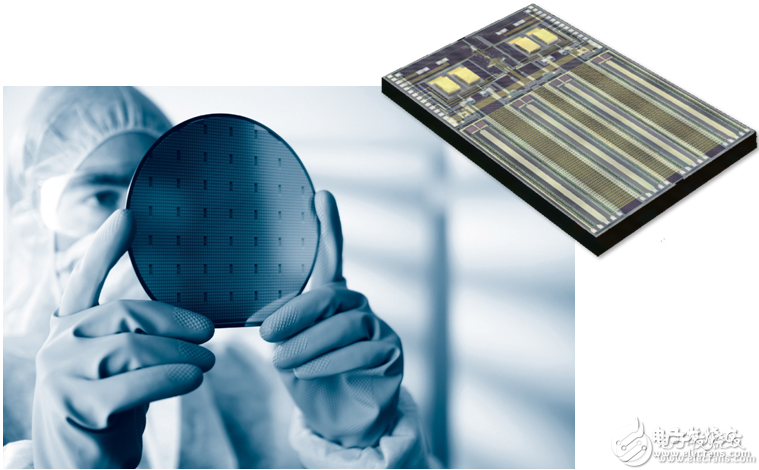
MAOP-L284CN-100G Quad L-PIC for Data Center
In some markets, EFT can have a disruptive impact and play a key role in achieving cost reduction and mainstream deployment. With the L-PIC portfolio, MACOM once again demonstrates the significant advantages of EFT and leads the cloud data center toward high-speed, energy-efficient optical interconnects at 100G and higher.
High Speed Blender,Ipl Laser Hair Removal,Diy Laser Hair Removal,Best Ipl Hair Removal,Epilator Ipl
SHENZHEN CHONDEKUAI TECHNOLOGY CO.LTD , https://www.szfourinone.com