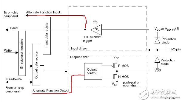
The stm32 pin has two uses: GPIO (general purpose io) and AFIO (alternate funcTIon io)
For some pins (depending on the chip), neither of these two uses, as in 64-pin products, OSC_IN/OSC_OUT shares the same pin as PD0/PD1 as GPIO port, and in 100, 144 pin products In the above, these four functions have corresponding pins and do not conflict with each other. Therefore, OSC_IN/OSC_OUT does neither GPIO nor AFIO. Of course, such pins are not the focus of discussion.
1, the configuration of the pin
Whether for GPIO or AFIO, configure the pins. In the firmware library function, using the GPIO_Init() function to configure the pin does not mean that this function has the word "GPIO" to be used as a GPIO. Instead, it is included in the scope of GPIO for discussion.
The so-called configuration is the on-chip resource connection on the pin, such as pull-up resistors, mitr triggers, and so on. Understand the configuration, you can understand the difference between configuration and mode.
Specifically, push-pull and open-drain in the output configuration will be discussed in detail below.
2, multiplexing function
There are two kinds of multiplexing functions: no re-imaging, re-imaging (including partial re-imaging, full re-imaging), use of pins as AFIO functions, and they also need to be configured.

These three sentences come from the reference manual, but I have questions about the first sentence and the attention, and the third tells. If the port is configured as a multiplexed output function, the pin is disconnected from the output register and connected to the on-chip peripheral's output signal. The input configuration is not different from GPIO.
Why does the output mode have a special multiplexing mode and the input does not. Because the output is driven by the internal circuitry of the chip, it must select which peripheral the driver is coming from, whether it is a GPIO or another peripheral that multiplexes this pin, that is, select which external device the pin is connected to internally. Explain that this will cause signal confusion. The input is different, the input signal is driven by the signal outside the chip, although the signal may have different directions after entering the chip, but do not need to configure this, because there will be no signal conflict, the worst case It is more than a register driven. In fact, when the pin is used as a GPIO input, the corresponding AFIO peripheral is in the off state and does not consume power; when the pin is used as an input to AFIO, the GPIO may not be read in. This is my Guess, there is no verification, can read it does not matter, do not have to tangled in this.
If multiplexing is selected, the default is no re-imaging, and the peripherals can be used directly, and no software setting is required.
But if you want to remap, you need to simply set it.
First configure the corresponding pin after remapping. Refer to the reference manual or the pin definition section of the data sheet to enable the AFIO clock and enable remapping. For example, remap USART1. The entire code is as follows:
RCC_APB2PeriphClockCmd(RCC_APB2Periph_AFIO, ENABLE);
/* Before reading and writing the AFIO_EVCR, AFIO_MAPR and AFIO_EXTICRX registers, the AFIO clock should be turned on before remapping and selecting the external interrupt line.
/* Configure USART1 Tx (PA.09) as alternate funcTIon push-pull */
GPIO_InitStructure.GPIO_Pin = GPIO_Pin_6;
GPIO_InitStructure.GPIO_Mode = GPIO_Mode_AF_PP;
GPIO_InitStructure.GPIO_Speed ​​= GPIO_Speed_50MHz;
GPIO_Init(GPIOB, & GPIO_InitStructure);
/* Configure USART1 Rx (PA.10) as input floaTIng */
GPIO_InitStructure.GPIO_Pin = GPIO_Pin_7;
GPIO_InitStructure.GPIO_Mode = GPIO_Mode_IN_FLOATING;
GPIO_Init(GPIOB, & GPIO_InitStructure);
GPIO_PinRemapConfig(GPIO_Remap_USART1,ENABLE);
This completes the configuration and remapping of the IO port, and the associated peripherals (USART1) can then be used again.
The external interrupt line can also be mapped, and need to open the AFIO clock, do not use GPIO_PinRemap function, use GPIO_EXTILineConfig to remap the pin to the interrupt line. In fact, rather than mapping, it is better to say that the selection pin is connected to the external interrupt line.
Remapping is not arbitrary and can only be remapped to the specified pin.
3, on the second quarter, that question, why can not be configured as analog input? What is the difference between analog input and floating?
The answer is that it can be configured as an analog input. The official firmware version 3.5 firmware example and the aligetek example both configure the ADC input pin as GPIO_Mode_AIN.
Then configure it into a floating line, but also ADC?
// routines
GPIO_InitStructure.GPIO_Pin = GPIO_Pin_0;
GPIO_InitStructure.GPIO_Mode = GPIO_Mode_AIN;
GPIO_Init(GPIOC, & GPIO_InitStructure);
//modify
GPIO_InitStructure.GPIO_Pin = GPIO_Pin_0;
GPIO_InitStructure.GPIO_Mode = GPIO_Mode_IN_FLOATING;
GPIO_Init(GPIOC, & GPIO_InitStructure);
Experiments show that both of these configurations can implement the ADC. Then the USART's Tx should be configured as GPIO_Mode_IN_FLOATING. If configured as GPIO_Mode_AIN, can it accept data? The results of the Jinniu board experiment are not, and ST is not bullied by me. In short:
Pins can be configured as analog inputs, using corresponding multiplexing functions;
The two configurations of floating and simulation are different.
Regarding the "attention" in the second quarter, I do not know what it means. My guess is this: Open a peripheral, this peripheral will take a pin as input, we have to configure this pin as GPIO output, so that you can operate GPIO to "cheat" this peripheral, this usage should be very delicate.
4, push-pull and open-drain
Not only does stm32 have this configuration, in fact, both of these have been widely used in many applications.
Push-pull, also known as push-pull, is a very visual name. It generally refers to the control of two transistors (MOS transistors) with two complementary signals (or one signal, but with complementary pairs of tubes), which are always turned on in one transistor. At the other end of the time, such circuits are called push-pull (complementary):
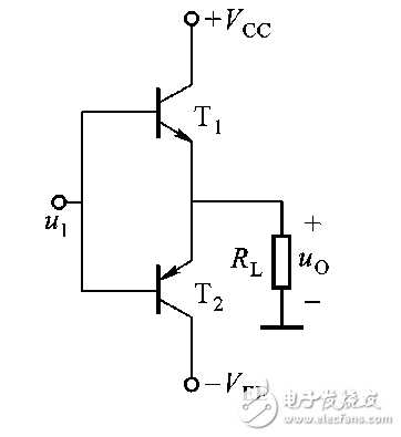
This circuit is usually used as an output stage in amplification. In STM32, this is the push-pull configuration.
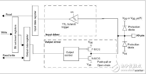
In the corresponding position 1, the P-MOS conducts and the N-MOS is turned off, and the output voltage is VDD. When the corresponding position is 0, the N-MOS is on, the P-MOS is off, and the output voltage is VSS. This is called push-pull. . It is relatively simple.
The so-called open-drain (for triodes is an open set, the same principle), it must be clever. The so-called "drain" in the so-called open drain circuit concept refers to the drain of a MOS FET. Similarly, the “set†of the open collector circuit refers to the collector of the transistor. The open drain circuit refers to a circuit that outputs the drain of a MOS FET. The general usage is to add a pull-up resistor to the external circuit of the drain. The complete open-drain circuit should consist of an open-drain device and an open-drain pull-up resistor.
For stm32, open drain is disabled P-MOS, so that when the corresponding position 1, the pin is actually in a floating state, and pull it up through an external pull-up resistor.
This has the following benefits:
1. Multiple open-drain outputs can be connected to one line. Form a "logical" relationship. When any one of the pins goes low, the logic on the open drain line is zero. This is also the principle of the I2C, SMBus, etc. buses to determine the bus occupancy status. This problem is also mentioned in my article "Stm32 Analog iic - Pin Configuration, Code".
2. It is possible to change the transmission level by changing the voltage of the pull-up power supply. In this way, we can use the low-level logic to control the output high logic. Imagine that the original stm32 output 3.3v voltage with IRF540 does not move directly to determine the re-selection, is the wrong idea, as long as the push-pull output into open-drain, plus pull up to 5v resistance, can solve this problem.
By the way, the resistance of the pull-up resistor determines the speed of the edge of the logic level transition. The larger the resistance, the lower the power consumption and the lower the power consumption. vice versa.
E-cig as a substitute of tobacco mainly reminds people of its potential benefits for health. Four ingredients contain in the e-liquid : propylene glycol, glycerin vegetable, nicotine and food grade essence. Nevertheless, smoke from cigarette contains carbon monoxide, tar, arsenic, ammonia, and many other cyanide and acetone.
Advantage
- New ceramic self heating element, Uniform heating
- High reduction, Temperaturecan be accurately controlled
- Safety and Health, Worth a product,Natural and realistic taste,Factory Direct Sale
- Using proprietary technology,Quality assurance, trustworthy
- Oil leakage free, compact, pocket-sized, portable and easy to transport
-
So that smokers can smoke addiction, refreshing, to meet the psychological and physiological needs of smokers, and in line with the habit of smokers for many years.
-
Compared with rechargeable e-cigarettes and mechanical e-cigarettes, the price of disposable e-cigarettes is much lower, which is applicable to a wider range of customers than the first two. It is also the absolute truth for ordinary consumer groups to be cheap.
Wax Device Oem,Thc Wax Device Oem,Marijuana Wax Device Oem,High Cost Performance Wax Device
Shenzhen MASON VAP Technology Co., Ltd. , https://www.disposablevapepenfactory.com