The new growth point of today's semiconductor integrated circuits (IC) has shifted from the traditional computer and communication industries to portable mobile devices such as smart phones, tablet computers and new-generation wearable devices. There are also new trends in integrated circuit packaging technology to cope with the special requirements of mobile device products, such as increasing functional flexibility, improving electrical performance, thinning the volume, reducing costs, and quickly becoming available.
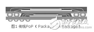
Package-on-Package (PoP, Package-on-Package, see Figure 1) is one of the very popular three-dimensional stacking technologies developed for the IC packaging of mobile devices that can be used for system integration. The PoP is formed by superimposing two upper and lower packages, and the interconnection between the bottom package and the upper package and between the bottom package and the motherboard (Motherboard) is realized through an array of solder balls. Usually, the system company purchases the bottom-layer package components and the upper-layer package components separately, and solders them together during the system board assembly process. The bottom package of the stack package is generally a baseband component, or an application processor, etc., while the upper package can be a memory, etc.
Compared with the traditional three-dimensional chip stacking technology, although the PoP structure size is slightly larger, the system company can have more component suppliers, and because the bottom and upper components of the PoP have passed the packaging test, the yield rate is guaranteed, so the PoP's System integration not only has flexibility in the supply chain, but also has the advantage of cost control. Facts have proved that PoP provides a low-cost solution for system integration.
In order to further utilize the advantages of PoP technology, system companies can cooperate with chip suppliers and packaging companies to further integrate PoP bottom or upper components to meet their product needs. For example, the baseband chip and the application processor chip can be integrated in the bottom package of the PoP.
With the further improvement of integration and electrical performance requirements, as well as the demand for ultra-thin, PoP packaging technology has also continued to develop and innovate, and has begun to enter a new generation. This article will introduce and analyze the latest development trends in this field.
The further ultra-thin packaging technology makes the package warpage a major problem. Various materials are used in the package, such as chips, substrates, plastic packages, etc. These materials have different coefficients of thermal expansion (CTE, Coefficient of Thermal Expansion). When the entire package undergoes temperature changes, for example, from the high temperature during the packaging process to room temperature, due to the different thermal expansion coefficients of various materials, the expansion and contraction are inconsistent, which causes the package to warp. Figure 2 simply illustrates this principle. When the package becomes thinner, the rigidity is significantly reduced, it is easier to deform, and the warpage is significantly increased.
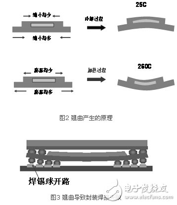
Excessive warpage will make the PoP package in the surface soldering (SMT) assembly process, the solder balls between the bottom package and the mother board, or between the bottom and upper packages cannot be connected, and an open circuit appears, as shown in Figure 3.
Warpage has become a key factor affecting PoP assembly yield. The trend of ultra-thinning has made the warpage problem more prominent, and has become a bottleneck hindering the development of future PoP thinning. Therefore, a variety of new technologies and materials continue to appear to reduce the warpage of the package. In this article, we will introduce the development trend of warpage control. The article further analyzes and discusses the possible warpage of ultra-thin PoP from a set of ultra-thin PoP test samples and some other actual product data, as well as the corresponding design, material, and production process possibilities brought by ultra-thin packaging. Problems and challenges that arise.
2 The development trend of package on package (PoP)The development trend of the new generation of package-on-package can be summarized as follows:
IC integration is further improved, chip size continues to increase, and the ratio of chip size to package size continues to increase, resulting in an increase in package warpage.
The electrical performance requirements of the package are further improved, and the application of flip chip technology (flip chip) has become popular, which has replaced the traditional wire bond technology. More advanced uses copper pillar technology (Copper Pillar) to further reduce the solder joint pitch.
The same chip adopts different package sizes for different applications and customer requirements. This allows the packaging materials to be changed and optimized accordingly. On the other hand, sometimes in order to improve IC manufacturing yield and output rate, or application flexibility, customers will divide a large integrated system chip into several small chips, but still require packaging in the same package. All of these make it difficult for the package to use the traditional unified material system, and it must be customized and optimized.
The pitch between the bottom and upper layers of the PoP is reduced. The traditional PoP uses 0.5 mm or more pitch, and now more uses 0.4 mm pitch. In the near future, 0.3 mm pitch will appear. The shrinking of the pitch causes problems with the solder height of the upper and lower interconnections. Traditional PoP uses solder balls as the interconnection between the upper and lower layers, and relies on the surface tension of the solder balls in the reflow liquid to form the height of the solder balls. This height must be greater than the thickness of the underlying package chip and plastic packaging, otherwise there will be open solder balls. In the case of reduced pitch and reduced solder ball diameter, this height requirement is difficult to achieve, and new technologies must be developed.
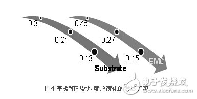
Under the trend of ultra-thinness, the thickness of each layer of PoP package is required to be thinner and thinner. Figure 4 shows the thinning trend of the thickness of the substrate and the plastic package (EMC). The thickness of the substrate has been reduced from the usual 0.3 mm to about 0.2 mm, or even 0.13 mm. The thickness of the plastic package is reduced from 0.28 mm to 0.2 mm and 0.15 mm. As for the chip itself, the thickness has reached 0.1 mm or less, and a 0.05 mm chip will also appear. The biggest problem caused by package thinning is the significant increase in package warpage. The development of many new POP technologies and the application of new materials are also aimed at reducing package warpage.
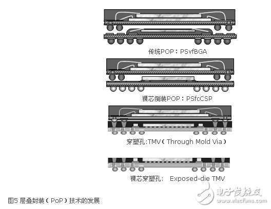
In packaging technology, bare core flip-chip bottom packaging (PSfcCSP) and through-mold-via technology (TMV, Through-Mold-Via) have emerged one after another, as shown in Figure 5. The warpage of the bare core flip chip is generally larger. Plastic hole technology makes up for this shortcoming. Plastic-through hole technology is based on the traditional plastic packaging. Holes are punched through the plastic packaging at the interconnection welding points of the upper and lower packages, and then the upper and lower layers are connected through the solder ball pillars. Plastic hole technology has some significant advantages. First of all, it can reduce package warpage through plastic packaging materials, and can use a higher chip/package size ratio, which makes it possible to package larger chips. Secondly, the solder balls of the upper and lower package interconnections can use a finer interconnection pitch because of the support and spacing of the plastic package.
In order to further thin the TMV plastic encapsulation layer, there is now a bare core TMV (Exposed-die TMV), that is, the height of the plastic encapsulation layer is designed to be flush with the chip, so that the top of the chip is exposed. In this way, the height of the entire package can be further reduced, but the warpage will be relatively increased.
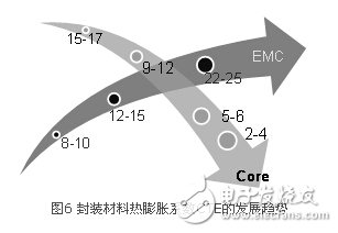
In order to reduce package warpage, a variety of new materials are also emerging, mainly in the improvement of material characteristics. Figure 6 shows the development trend of the thermal expansion coefficient (CTE) of the substrate core (Core) and plastic package (EMC). In terms of substrates, a substrate core with a low coefficient of thermal expansion is beneficial to reduce the warpage of a large chip package. Therefore, the coefficient of thermal expansion of new substrate core materials is continuously decreasing. The original standard substrate core thermal expansion coefficient is generally around 15-17 ppm, and then a low-CTE substrate core with a CTE between 9-12 ppm has appeared. Now the ultra-low substrate core with a CTE between 5-7 ppm has become quite popular. The latest generation is close to 2-4 ppm. At the same time, the CTE characteristics of plastic packaging materials continue to rise, and various high-CTE plastic packaging materials are emerging in an endless stream. The CTE value at room temperature has risen from the original 10 ppm to between 20-30 ppm. The development of these new materials has greatly helped to improve the warpage caused by thinning.
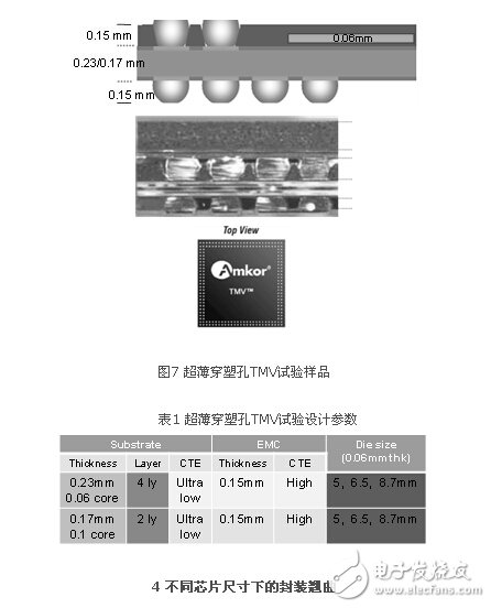
In order to explore the possible warpage of the package after ultra-thin packaging, as well as the corresponding design, material, and production process problems and challenges that may occur due to ultra-thin packaging, we designed and actually assembled a set of ultra-thin TMV test samples , See Figure 7.
Table 1 lists the experimental design parameters. The chip thickness is 60μm, and the corresponding plastic encapsulation layer thickness is 0.15 mm thick. Two substrate designs were used: one was a 4-layer board with a total thickness of 0.23 mm, and the other was a 2-layer board with a total thickness of 0.17 mm. The entire package size is 12 mm. In order to study the influence of different chip sizes on warpage, we used three chip sizes from small to large, namely 5 mm, 6.5 mm, and 8.7 mm. In the use of materials, an ultra-low CTE substrate and a high CTE plastic package combination are used.
Figures 8 and 9 respectively show the warpage values ​​when using a 4-layer 0.23 mm substrate and a 2-layer 0.17 mm substrate to package different size chips. These warpage values ​​are average values ​​measured by a shadow moiré. According to industry practice, a positive value of warpage means that the warpage is convex, and a negative value of warpage means that the warpage is concave, as shown in the figure.
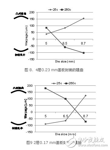
From the data in the figure, we can draw some very important conclusions:
After the package is ultra-thin, the warpage is very sensitive to the chip size. The warpage of different sizes of chips after packaging is very different, and even the direction of warpage will change. For example, the warpage at the reflow temperature of 260℃ in Figure 8, when the chip is 5 mm, the warpage direction is convex positive 90μm (positive When the chip is 8.7 mm, the warpage becomes concave minus 100μm (negative value).
For large chips (8.7 mm), the warpage of the ultra-thin package is very large, exceeding the general required warpage level (below 100μm). Therefore, the warpage of large chip ultra-thin packages is extremely challenging. On the other hand, it does not mean that the smaller the chip, the smaller the warpage. If the design or material selection is not appropriate, the small chip package will have more warpage than the large chip package. For example, as shown in Figure 9, the warpage of the 5 mm chip is larger than that of the 6.5 mm and 8.7 mm chips. The reason is that the direction of warpage of chips of different sizes may be different.
Generally speaking, the combination of a low-CTE substrate and a high-CTE plastic package is beneficial to reduce warpage. It is true when the warpage direction is convex at room temperature and concave at high temperature when packaging large chips. When small chips are used, the direction of warpage may be reversed. At this time, the above point of view will no longer hold. Instead, a high-CTE substrate and a low-CTE plastic package combination must be used to reduce warpage.
The data in the figure shows that the same material combination and design is difficult to apply to chips of different sizes.
To sum up, the new generation of ultra-thin packages will cause various possibilities for warpage size and direction, and they are quite sensitive, making it difficult to predict based on experience alone. Therefore, it is necessary to customize and optimize, and use the relevant computer finite element warpage model simulation simulation in the design to help estimate the warpage of the final package and the improvement plan such as the selection and matching of the thickness of each layer and the material.
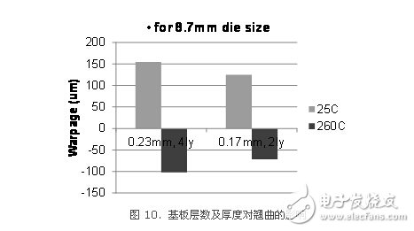
5 The effect of substrate thinning on warpageWhen designing the substrate, different layers and thicknesses can be selected. In addition to the consideration of the electrical properties of the substrate, these factors also have an impact on the warpage of the package. Figure 10 shows the difference in warpage between a package with a 4-layer board and a 2-layer board. For large chip packages, the warpage of the package using a 4-layer substrate will be greater than that of a 2-layer substrate. This is because the 4-layer substrate contains more metal layers and insulating layers. These materials have a relatively high CTE, so that the effective CTE value of the entire substrate of the 4-layer substrate is larger than that of the 2-layer substrate, and the warpage increases accordingly. . In contrast, the more the number of substrate layers, or the thinner the substrate core, the smaller the role of the substrate core, and the greater the warpage. By analogy, package warpage using the latest coreless substrate (Coreless Substrate) will be a greater challenge.
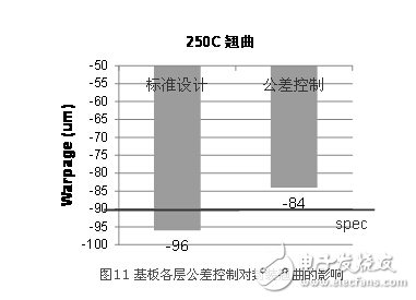
Another problem brought about by the thinning of the substrate is the increase in the influence of the tolerance of the substrate design. Traditional substrates use very thick cores, which play a leading role in the mechanical properties of the entire substrate, so the influence of design tolerances is not obvious. However, when the substrate becomes thinner, the leading role of the core becomes weaker, and the difference in the finished substrate caused by the design tolerance of the thickness of each layer can no longer be ignored. Figure 11 shows an example of the influence of tolerance control in substrate design. The first set of data adopts the standard design and the total difference. As a result, the warpage of the package is 96μm at reflow high temperature, which exceeds the customer's index (90μm). The second set of data is an improved version, which further controls the thickness tolerance of each layer of the substrate, especially the metal layer (signal layer). As a result, the warpage of this group was improved, reduced by 12μm, and reached the customer's target requirements. This shows that when the substrate becomes thinner, the tolerance control must be strengthened. At the same time, when the package product development has entered the final stage and various other parameters have been finalized, it is also possible to optimize the thickness tolerance of each layer of the substrate. Control to further improve the warpage and achieve customer targets.
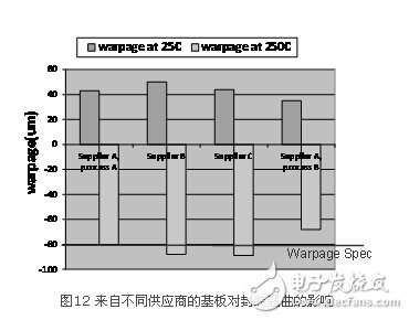
Based on similar reasons, we found that after the substrate becomes thinner, the difference in the finished substrate caused by the difference in the production process control of different substrate manufacturers has become more obvious, and more stringent control must be applied [6]. Especially in the modern business model, the same substrate is always purchased from several different suppliers. Figure 12 shows an example of the effect of substrates of the same design but from different suppliers on the final package warpage. The data shows that the warpage of packaging using the substrates of the three suppliers is different, with a difference of up to 20μm. Among them, the warpage of the substrate packages of suppliers B and C eventually exceeded the standard. Even if it is the same supplier A, different production process control will cause warpage differences.
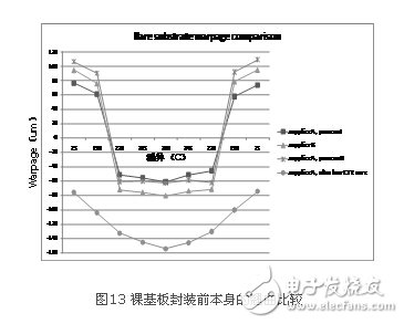
To further study the root cause of the substrate differences, we also measured the warpage of each unit of the bare substrate of these substrates before packaging. Figure 13 shows a comparison of the warpage of bare substrates from different suppliers before packaging. It can be seen that after the substrate is thinned, it is no longer as flat as the traditional thick substrate, and the bare substrate itself will produce a lot of warpage (up to 100-200μm), and the warpage varies with different suppliers and different productions. Process control is different. Another finding is that the warpage of the bare substrate itself can show completely different states with different substrate core materials.
The warpage of the bare substrate itself not only affects the warpage of the final package, but also affects the manufacturability of the packaging process. For example, in the chip flip process, if the bare substrate warps too much, the chip flip cannot be implemented.
After the package is thinned, the substrate becomes more sensitive to design tolerances and differences in supplier production processes. Therefore, stricter tolerance control and supply chain control must be adopted to better control the warpage of the final package.
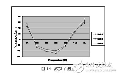
6 Warpage of ultra-thin bare chipsThe chip itself is also continuously thinning, from 100μm to 80μm, 60μm, or even below 50μm, and the warpage of the chip itself has also begun to appear. Figure 14 shows the warpage of a bare chip with a thickness of 50μm and a size of 8 mm×8 mm at different temperatures. The data in the figure shows that the warpage of a 50μm thick chip itself can be changed from positive 50μm (convex) at room temperature to minus 40μm (concave) at high temperature 260°C. This degree of warpage is still significant. It should be noted that the warpage of the chip itself will also vary due to different designs and manufacturing processes, and cannot be generalized.
The warpage of the ultra-thin chip itself is mainly caused by the different coefficient of thermal expansion between the silicon crystal and the subsequent low-k layer (BEOL). When the chip is thick, the silicon crystal is not easy to be deformed due to its high rigidity, but when the chip is very thin, the rigidity is significantly reduced and the warpage is also significantly increased.
The warpage of the chip itself will increase the difficulty in the assembly process, and the yield of the chip flip-chip process will also affect the warpage of the final package.
This article discusses the development trend of a new generation of package-on-package (PoP). Mainly manifested in the increase of the chip/package ratio, the application of flip chip and copper pillar technology, the reduction of the interconnect spacing between the upper and lower package layers, and the ultra-thin package. For this reason, new PoP technologies such as through-hole TMV have been developed, and a new generation of ultra-low CTE substrates and ultra-high CTE plastic packaging materials have also been developed rapidly to reduce package warpage caused by ultra-thinness. The article further discussed package warpage, which has become a bottleneck problem and challenges that hinder the development of a new generation of PoP. Based on the collected production experiment data, the following conclusions can be drawn:
The package warpage after ultra-thin is very sensitive to the chip size.
The thickness design of each layer of the package and the selection of packaging materials must be customized and optimized according to different applications and different chip sizes. Different combinations can be used to control warpage. It is difficult to reuse the traditional development model of the same material configuration suitable for different product designs.
After ultra-thin, the design tolerance of the substrate and the difference in the production process of different suppliers have more significant effects on package warpage. Therefore, it is necessary to adopt more stringent tolerance control and supply chain control.
The ultra-thin chip will also cause significant warpage of the bare chip itself.
Titanium Sunglasses,Eyewear Titanium,Titanium Frame Sunglasses,Sunglasses With Titanium Frames
Danyang Hengshi Optical Glasses Co., Ltd. , https://www.hengshi-optical.com