As the density of electronic components on the PCB board is getting higher and higher, the traces are getting narrower and the frequency of the signal is getting higher and higher, it will inevitably introduce EMC (electromagnetic compatibility) and EMI (electromagnetic interference) problems, so the electronic The electromagnetic compatibility analysis of products is particularly important. Compared with IC design, EMC analysis and simulation in the PCB design process are a weak link.
In PCB design, EMC/EMI mainly analyzes the signal integrity of the wiring network itself, the electromagnetic radiation and electromagnetic interference that the actual wiring network may generate, and the ability of the circuit board itself to resist external electromagnetic interference, and proposes layout and wiring according to the requirements of the designer The rules for suppressing electromagnetic radiation and interference are used as the guiding principles for the entire PCB design process.

Specifically, signal integrity analysis includes reflection analysis of the same signal on the same wiring network, impedance matching analysis, signal overshoot analysis, signal timing analysis, signal emphasis analysis, etc.; for the crosstalk analysis between different signals on adjacent wiring networks. In the signal integrity analysis, the geometric topology of the wiring network, the dielectric characteristics of the PCB insulation layer and the electrical characteristics of each wiring layer must also be considered.
The electromagnetic radiation analysis mainly considers the electromagnetic radiation at the interface between the PCB board and the outside, the electromagnetic radiation of the power layer in the PCB board, and the external radiation problem during the dynamic operation of the high-power wiring network. If the circuit design uses a heat sink that is tied to a high-power IC (for example, a metal heat sink attached to the Pentium processor), then such a heat sink will continuously radiate electromagnetic waves outward like an antenna in the dynamic circuit work, so Must be listed as the focus of EMC analysis.
Now there are international standards for suppressing EMI of electronic equipment and instruments, collectively referred to as electromagnetic compatibility (EMC) standards. They can be used as guidelines for ordinary designers to suppress electromagnetic radiation and interference during wiring and layout. For designers of military electronic products , The standard will be stricter and the requirements will be more demanding.
For the design of high-speed digital circuits, especially when the digital signal rate on the bus is higher than 50MHz, the use of lumped parameter mathematical models to analyze EMC/EMI characteristics seems incapable in the past. Designers tend to use distributed parameter mathematical models for wiring networks. Transmission line analysis (TALC). For an electronic system formed by connecting multiple PCB boards through a bus. The electromagnetic compatibility performance between different PCB boards must also be analyzed. EMC/EMI component library support
Nowadays, a circuit board may include hundreds of electronic components from different manufacturers with different functions. The designer must understand the electrical characteristics of these components in order to conduct EMC/EMI analysis, and then perform specific simulations. This seemed to be a difficult task in the past. Now, thanks to the support of databases such as IBIS and SPICE, the problem of EMC analysis is easily solved.
In view of the data models of SPICE3, HSPICE, and PSPICE that are already well known to the majority of circuit designers, IBIS will be introduced here. IBIS (I/O Buffer Interface Specification), namely ANSI/EIA-656, is a model that quickly and accurately describes the electrical performance of the I/O buffer based on the V/I curve obtained through measurement or circuit simulation. In 1990, INTEL led the joint establishment of the IBIS V1.0 industry standard with several well-known semiconductor manufacturers. After continuous improvement and development, it was updated to IBIS V3.0 in 1997.
Now this standard has been supported by hundreds of semiconductor manufacturers such as NS, Motorola, TI, IDT, Xilinx, Siemens, Cypress, VLSI, etc. At the same time, RDA companies such as Cadence, Mentor, Incases, Zuken-Redac have also added relevant information in their software. The functional module of IBIS.
The IBIS file is a text file, which is a description of "behavior" information generated through a standard software format to illustrate the analog electrical characteristics of the IC. Most IBIS modules are derived from the SPICF model, and the model can also be described by the actual measured V/I curve. The SPICE model of IC is a trade secret based on the foothold of various semi-public players and is protected by intellectual property rights, while the IBIS model is data that is completely open to users, so designers can get these data for free. Most semiconductor manufacturers publish the IBIS data of related ICs on their own websites or on product CD-ROMs. Because EDA manufacturers and electronic component manufacturers jointly support data models such as IBIS and SPIICE, designers can use them for circuit simulation or EDA tools to easily perform EMC/EMI analysis.
Combination of EMC/EMI simulation and PCB design
In the past electronic circuit design, engineers mostly relied on years of development experience to solve the EMC problem in the process of hardware debugging or the whole debugging of electronic equipment after the PCB was made. This is obviously a qualitative, non-quantitative and unreliable , Inaccurate methods. Since the beginning of the 1990s, electronic products have been developing towards low power consumption, low electromagnetic radiation, miniaturization and light weight, and they are required to work in a complex and harsh environment. In order to shorten the product development cycle as much as possible, engineers have to create another New path.
A more ideal PCB design process is shown in Figure 1. EMC/EMI criteria are added in the layout and routing stage of PCB design. For example, in order to reduce the mutual crosstalk between parallel signal lines, it can be specified that the distance between the lines cannot be less than a certain value. In order to reduce the reflection of the signal, match the input and output impedance, and avoid the ringing phenomenon, the geometric topology of the wiring network, the length of the wiring, and even the resistance container (commonly used) The methods include connecting resistors in series, and connecting pull-up, pull-down or up-and-down resistors, and clamp diodes can also be used). After the PCB layout is completed, EMC/EMI analysis and simulation are performed on the circuit design before the actual circuit board is made. At the same time, the signal strength, time delay and other characteristics are analyzed according to the dynamic operating frequency of the actual circuit.
If the designed PCB contains an external interface, a heat sink is added to the IC or the circuit itself consumes a lot of power, further simulation analysis of electromagnetic radiation must be carried out. For high-speed circuits, it is necessary to analyze the distribution parameters of the TALC transmission line of the wiring network. These newly added steps in the design stage actually advance some of the previous hardware debugging work to the computer design platform to complete, and its superiority is obvious. Because of the support of databases such as IBIS and SPICE, the indefinite EMC/EMI analysis of the past has become an accurate and subtle calculation result that is slightly different from the actual measurement. The designer can avoid the disadvantage of poor electromagnetic compatibility of the product based on the results of the simulation.
EDA developers have gradually paid attention to the needs of users in the field of EMC/EMI simulation. The German INCASES company provides designers with EMC-WORKBENCH, a software package for EMC/EMI simulation analysis, and has become a leader in the industry and has hosted many times. IEEE seminar on EMC/EMI. EMC-WORKBENCH can meet the urgent needs of circuit designers in terms of electromagnetic compatibility, improve the process of PCB design, and simplify many complicated tasks in the later hardware debugging.
The internal layout and wiring of the IC must fully consider the EMC problem; many EPLD and FPGA software must analyze the EMC problem before generating the final fuse diagram; for the PCB that constitutes the electronic system, the electromagnetic compatibility and electromagnetic interference characteristics must be analyzed. Design principles are reaching consensus among more and more circuit designers. Because of EMC/EMI simulation, PCB design has entered a new era. Electronic engineers can use it to design high-quality and high-reliability products in a short period of time. The implementation of EMC/EMI simulation analysis will surely bring unlimited business opportunities to circuit designers and PCB manufacturing.
High Voltage Industrial High Bay Driver UFO
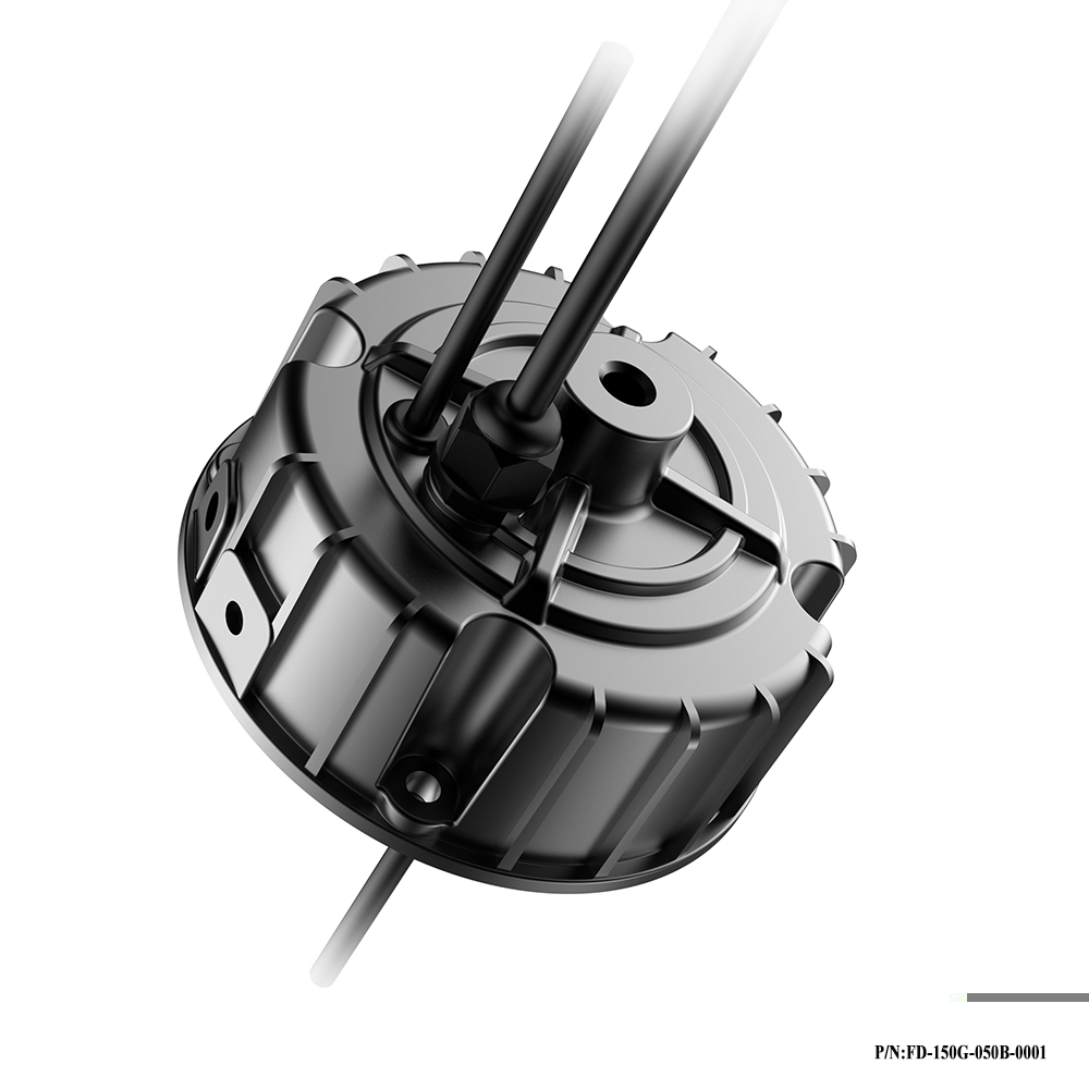
Fahold LTD -- Products Dept. has introduced a new series of 200-480V LED Round drivers, available in 100W,150W and 240W outputs.
Each model includes input voltage ranges from 200Vac to 480Vac. The FD-150GW constant current driver offers fixed and dimmable output models. Some models are Class 2 rated.
All models feature Metal housings and are IP65 rated--making them suitable for applications subject to moisture. They offer over-voltage, over-current and short circuit protection with automatic recovery to keep luminaires performing. it has the special heat dissipation design, wehich allow to work at Ta 65°C. The drivers are UL Recognized for both US and Canada, and are CE certified.

Industrial Lighting Led Driver,480V Constant Led Driver Circuit,UFO High Bay Lighting,Led Driver Power
ShenZhen Fahold Electronic Limited , https://www.fahold.net