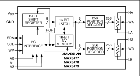
Download: GUI software (ZIP, 229kB) Overview Digital potentiometers have the advantages of high reliability, small size, and ease of use. They are widely used to replace mechanical potentiometers, especially in terms of volume control. The application is very common. Considering that the human ear's perception of volume attenuation is non-linear, logarithmic attenuation is regarded as linear attenuation. Therefore, audio equipment generally tends to use logarithmic digital potentiometers rather than linear digital potentiometers. If only high-resolution linear digital potentiometers are provided in the system, the linear potentiometer (Figure 1) can be converted into a logarithmic potentiometer in the following manner without changing the system hardware.

Figure 1. This series of digital potentiometers are equipped with a standard configuration, with high-end, low-end, and center-tap connection points of the resistance string. The position of the center tap can be moved along the resistance string.
Logarithmic adjustment with a linear potentiometer The use of a simple and easy-to-understand linear-tap digital potentiometer with a mathematical relationship can complete the function of a logarithmic digital potentiometer. Since the digital potentiometer is essentially a voltage divider circuit, its output voltage has a certain correspondence with the input voltage VIN (VIN acting on RH) acting on both ends of the potentiometer, which can be expressed by the following formula:
VOUT = VIN (RW-L / RH-L)


 (Formula 1)
 Among them, RW-L is the resistance value between the center tap (W) and the low end (L) of the resistance string, and RH-L is the total resistance between the two ends of the potentiometer.
Calculate the decibel number of voltage attenuation according to the following formula:
Attenuation (dB) = 20 * log (VOUT / VIN)


 (Formula 2)
 Substituting VOUT of equation (1) into equation (2), the following relationship can be obtained:
Attenuation (dB) = 20 * log [VIN (RW-L / RH-L) / VIN] = 20 * log (RW-L / RH-L)


 (Formula 3)
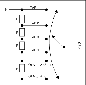
 As shown in Figure 2, the resistance value can be expressed by the position of the tap of the potentiometer (RW-L) and the total number of taps (RH-L).

Figure 2. The tap point of the linear potentiometer is at the position of the bisector string
The position of the potentiometer tap (RW-L) can be expressed as:
RW-L = (Total_Taps-x) * R


 (Formula 4)
 Where x = 1, 2, 3 ... Total_Taps, Total_Taps is the total number of taps.
Since the first tap point (minimum attenuation) contains no resistance, the total end-to-end resistance is: RH-L = (Total_Taps-1) * R, the attenuation can be expressed by the following formula:
Attenuation (dB) = 20 * log [(Total_Taps-x) / (Total_Taps-1)]


 (Formula 5)
 Where x
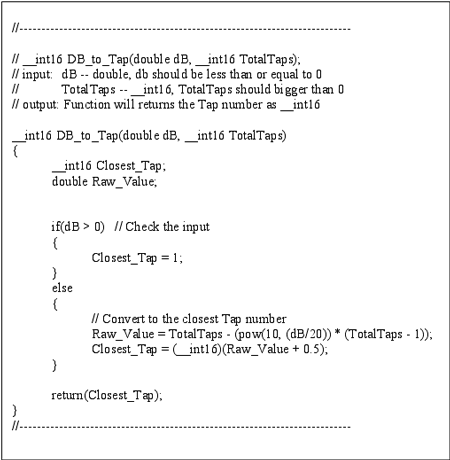
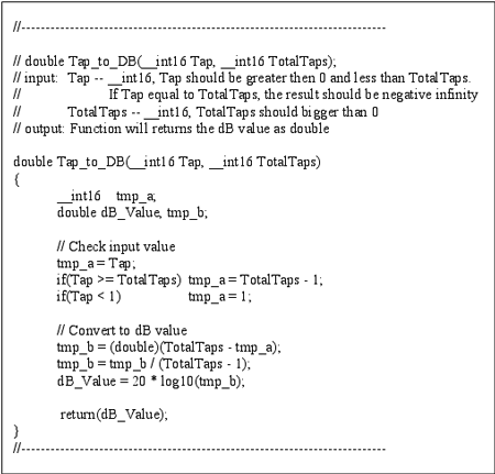
Conclusion It can be seen from the above analysis that it is completely feasible to convert a linear potentiometer to a logarithmic potentiometer. This method is very suitable for high-resolution linear potentiometers (128 taps or higher), because the resolution of the logarithmic potentiometer is strict Limited to the range of linear tap points (less than 128). In addition, due to internal structures such as the ESD protection circuit or the non-linear on-resistance of the transistor as a switch, accuracy may be affected at the end point. The program code given below can realize the conversion between the attenuation amount and the tap position (Figure 3) and the required tap position and attenuation (Figure 4).

Figure 3. This program is used to convert between attenuation and tap position

Figure 4. This program is used to convert between tap position and attenuation
A similar article was published on EE TImes on April 4, 2005.
Storm Circuit has been producing Multilayer PCBs for over 10years. Over the years, we have seen all types of multilayer constructions from various industries, answered all types of multilayer questions, and solved all types of problems with multilayer PCBs.
Multilayer PCB is a circuit board with two or more layers. The material unlike Double-Sided PCBs with only two conductive layers all multilayer PCBs is that it must have at least three layers of conductive material, and the PCB boards are buried in the center of the material.
Benefits of Multilayer PCBs (compared to single or double-sided PCBs)
Higher assembly density
Smaller size (considerable savings on space)
Increased flexibility
Easier incorporation controlled impedance features.
EMI shielding through careful placement of power and ground layers.
Reduces the need for interconnection wiring harnesses (reduces overall weight
Multilayer PCB
Multilayer PCB,Multilayer Bga Board,Multilayer Smd PCB,Multilayer Circuit Board PCB
Storm Circuit Technology Ltd , https://www.stormpcb.com