Recently, in the "2015 high-tech LED good product tour" Foshan station , Li Junzheng, deputy general manager of the research and development department of Guoxing Optoelectronics White Light Devices Division, said that the company introduced chip-level package (CSP) high-power LED devices, which are the most advanced in the industry. The ceramic film substrate (C-TFS) package architecture enables high-conventional packaging of LEDs for backlighting, high-density lighting, projection equipment, high-end indications, and more.
“No obvious leakage (about 0.3μA) was observed in the solder paste and the transition substrate structure. It is inferred that the stress generated by the material thermal expansion mismatch can easily damage the GaN layer and solidify through the solder paste (increasing the solid crystal). Thickness) or introduction of a transition substrate structure (thermal expansion of the ceramic substrate ~7ppm/K) can alleviate or block the conduction of stress to the GaN layer."
Guoxing Optoelectronics further confirmed the above inference through the thermal shock (-40 ° C ~ 100 ° C) experiment. The straight welded structure failed after 100 cycles, and the failure rate was as high as 70% after 300 cycles.
It is found that increasing the thickness of the solid crystal layer can inhibit the stress conduction, but its reliability still has a high risk. After 100 cycles, the failure also occurs. After 3000 cycles, the failure rate reaches 30%, and the ceramic transition substrate structure is entirely. The test maintains a 0 failure.
Li Junzheng said that the analysis results show that increasing the thickness of the solid crystal layer (An/Sn or solder paste, 3μm to 27μm) can significantly reduce the chip assembly stress, the stress of the die bond layer is reduced by 67.7%, and the stress drop of the GaN layer is even higher. 85.8% confirmed that it is feasible to increase the thickness of the solid crystal layer (usually achieved by solder paste solid crystal) to improve the reliability of the flip chip CSP package.
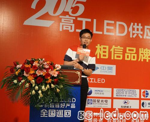
Li Junzheng, deputy general manager of R&D department of Guoxing Optoelectronics White Light Devices Division
“No obvious leakage (about 0.3μA) was observed in the solder paste and the transition substrate structure. It is inferred that the stress generated by the material thermal expansion mismatch can easily damage the GaN layer and solidify through the solder paste (increasing the solid crystal). Thickness) or introduction of a transition substrate structure (thermal expansion of the ceramic substrate ~7ppm/K) can alleviate or block the conduction of stress to the GaN layer."
Guoxing Optoelectronics further confirmed the above inference through the thermal shock (-40 ° C ~ 100 ° C) experiment. The straight welded structure failed after 100 cycles, and the failure rate was as high as 70% after 300 cycles.
It is found that increasing the thickness of the solid crystal layer can inhibit the stress conduction, but its reliability still has a high risk. After 100 cycles, the failure also occurs. After 3000 cycles, the failure rate reaches 30%, and the ceramic transition substrate structure is entirely. The test maintains a 0 failure.
Li Junzheng said that the analysis results show that increasing the thickness of the solid crystal layer (An/Sn or solder paste, 3μm to 27μm) can significantly reduce the chip assembly stress, the stress of the die bond layer is reduced by 67.7%, and the stress drop of the GaN layer is even higher. 85.8% confirmed that it is feasible to increase the thickness of the solid crystal layer (usually achieved by solder paste solid crystal) to improve the reliability of the flip chip CSP package.
LCD Tonch Screen For Iphone 12
Lcd Tonch Screen For Iphone 12,Lcd Touch Screen For Iphone X12Pro,Lcd Display For Iphone X12Pro,Mobile Lcd For Iphone X12Pro
Shenzhen Xiangying touch photoelectric co., ltd. , https://www.starstpmobile.com