A very wideband new RMS power detector solves many of the challenges for microwave design engineers to achieve accurate power measurements of complex modulated signals at microwave frequencies. The LTC5596RMS power detector has the following key advantages:
Â
  l   Wide input frequency range from 100MHz up to 40GHz (Ka band); full impedance matching to 50Ω without any external matching components.
35dB log-linear dynamic range within the temperature range I grades housing (- 40 ° C to + 105 ° C) having the accuracy of ± 1dB. Class H devices with operating temperatures up to 125 °C are also available .
Very flat frequency response; response shifts between 200MHz and 30GHz are typically less than ±1dB .
High output drive capability to drive 50Ω loads.
The high ESD rating (3.5kV HBM and 1.5kV CDM) makes it easy to handle in a production environment.
The response is very insensitive to large peak-to-average power ratios (PAPR) , making it ideal for accurate measurements of highly complex waveforms without the need for extensive calibration work.
Â
The LTC5596 's RF input is accurately impedance matched to 50Ω ( from 100MHz up to 40GHz) , as shown by the measured return loss in Figure 1 .
Â
Â
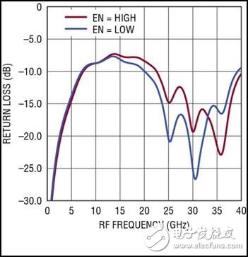
Figure 1 : Input return loss versus frequency
Â
Â
RF input "ground - signal - ground" configuration (FIG. 2) is designed with a seamless waveguide coplanar ground on a 5 mil thick substrate and RO3003 or similar design, it does not require any external matching components.
Â
Â
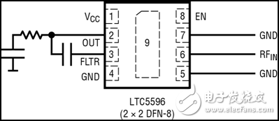
Figure 2 : LTC5596 pinout configuration and interface connection
Â
Â
In addition, the response of the LTC5596 has little change over a wide input frequency range. This minimizes the need for response calibration at different frequencies. 3, the measurement error due to the frequency response caused by dependence (with respect to 5.8GHz frequency response) of less than ± 1dB over the frequency range of 200MHz to 30GHz.
Â
Â
Â
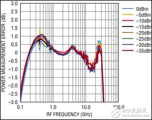
Figure 3 : Frequency dependence of detector response expressed as input power measurement error ( relative to 5.8 GHz)
Â
Â
By its very nature, the root mean square (RMS) power detector is ideal for accurately measuring the average power of an arbitrary waveform. This is because such devices accurately perform a defined formula for average power ( proportional to the average of the square of the signal ) . Other types of power detectors ( eg, Schottky diode detectors or demodulated log amps ) perform slightly different operations, which often involve signal envelopes. This causes a change in its response whenever the input waveform ( but not the average power level ) changes. New communication systems make extensive use of complex modulated high PAPR signals (OFDM , WCDMA) and adaptively adjust and code according to the quality of the ( radio ) link. This does result in thousands of different waveforms with widely varying PAPRs . In such an environment, the use of non- RMS power detectors to achieve the required power measurement accuracy ( typically ±1 dB) can often only be accomplished using a wide range of comprehensive and time consuming calibrations, as well as a priori knowledge of the received waveform type. When using the LTC5596 RMS power detector , such calibration is usually no longer necessary for signals up to the Ka -band frequency.
Â
In many applications, the power level of an RF signal is typically specified on a dB scale ( one of the motivations for this approach is that the transmission path loss is approximately log-linear versus distance ) . The LTC5596 produces a (DC) output voltage that is proportional to the average power level (rms signal level in dBm) on its input port . Further, in response to a wide operating temperature range it is very stable, so that an error is generally less than ± 1dB over the entire operating temperature range, as shown in FIG.
Â
Â
 Â

Figure 4 : Logarithmic linear response of LTC5596 at 30 GHz and error of ideal logarithmic linear transfer with respect to 25oC .
Â
Â
At any point in the LTC5596 - 37dBm to - 2dBm dynamic range, a 1dB change in input power results in a 29mV output voltage change. For example, for a 1 dB power step, a diode type detector or a voltage linear power detector produces an output signal change at a high power level that is much smaller than the output signal change produced at a low power level. This makes it very difficult to achieve sufficiently accurate power measurements over the entire dynamic range. By connecting an ADC to the LTC5596 output, a digital representation of the measured power with constant and high resolution is obtained over the entire dynamic range.
Â
In addition, the LTC5596 provides an easy way to perform additional filtering on the output signal, which is suitable for reducing residual high frequency ripple and noise. A single capacitor connected between OUT and FLTR can be easily utilized to reduce the bandwidth of the output driver amplifier inside the device without sacrificing the current drive capability of the device. It is usually sufficient to use tens of pF capacitors. Alternatively, you can connect a filter to the OUT interface of the device . The high drive capability of the LTC5596 allows for a wide range of impedances without changing the power measurement accuracy. The LTC5596 is ideal for low duty cycle applications where the device is only running for a fraction of the time. The output interface changes to high impedance during shutdown mode, which minimizes the discharge of large capacitors in the output filter and ensures fast stabilization once the device is re-enabled.
Â
LTC5596 of Class I (- 40 ° C to 105 ° C housing temperature) and H (- 40 ° C to 125 ° C housing temperature) device is a small 2x2 DFN-8 package. Class H devices guarantee tighter limits on their log slope and intercept parameters, which simplifies or even eliminates the need for factory calibration.
docking station for macbook air,docking station for laptop,docking station usb c,USB C HUB,thunderbolt 3 usb type c hub
Shenzhen Konchang Electronic Technology Co.,Ltd , https://www.konchangs.com