In many different applications, engineers often face the challenge of verifying, debugging, or analyzing digital signal behavior. The digital signal is superimposed by a series of analog signals with high frequency sinusoidal components and forms edges with differentiated digital values. The challenge of measuring these signals is that if a simpler measurement is made without careful understanding and consideration of various aspects of the measurement, the results provided may be incorrect.
This article discusses the basic principles of measuring high-frequency digital signals in a typical digital subsystem and how to obtain the best and most reliable results to analyze the signal integrity of the system.
Hypothesis
Because of the extensive knowledge of digital system knowledge, this article assumes that you are familiar with the following concepts: digital signals, impedance matching, transmission lines, digital signal termination, and oscilloscopes. In addition, it is assumed that all interconnections (cables) have a 50Ω characteristic impedance.
Basic knowledge of measuring signal integrity in digital systems
To introduce the concept of measuring the signal integrity of a digital system, we will evaluate a basic digital signal measurement as if the oscilloscope were part of the system. This means that the output of the digital line is directly connected to the oscilloscope via an accessory:

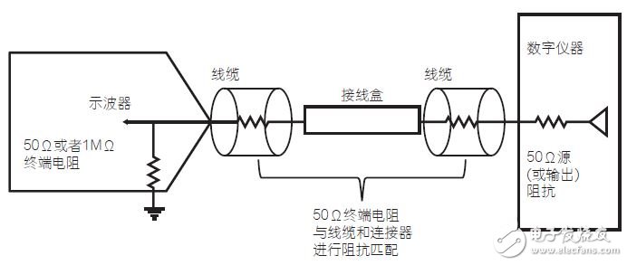
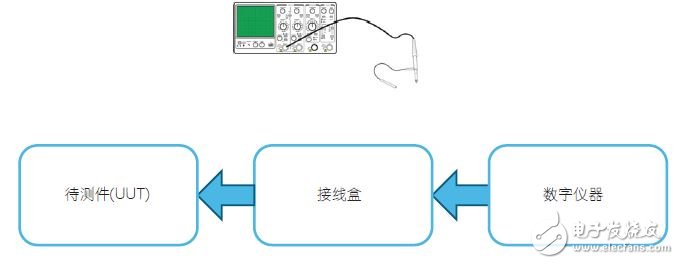
Figure 1: The oscilloscope is connected in series with the digital output of the digital instrument. The two instruments are connected via a VHDCI to SMB junction box. This common condition can be used to verify the signal integrity of the accessory terminal output.
In this case, the oscilloscope is at the end of the transmission line, which means the signal is terminated with the oscilloscope. If the oscilloscope is terminated with 1MΩ, it means that the square wave signal will be completely reflected back to the transmitter. If a 50Ω termination is used, there will be no reflected signal and the oscilloscope senses the voltage by half. This voltage drop is due to the fact that when the AC signal reaches the 50Ω source impedance at the transmitter through the 50Ω characteristic impedance cable, a 50Ω voltage divider circuit is formed.

Figure 2: Schematic diagram of the apparatus of Figure 1.
The resulting measurement will accurately display the digital signal at the end of the transmission line received by the UUT. Below are a variety of different probing scenarios.
Measuring digital signal integrity using a parallel-connected oscilloscope
A more complicated scenario is to try to measure the integrity of a digital signal when the oscilloscope is not terminating the signal. In this scenario, a square wave is generated by a digital instrument and input into the device under test. We want the oscilloscope probe to be connected in parallel with the data transmission to view the signal as it propagates through the transmission line medium:

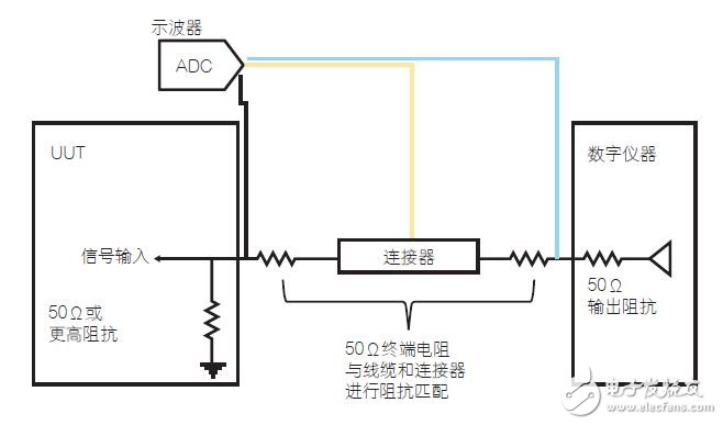
Figure 3: Schematic diagram of an oscilloscope probe measurement on the system. The probes are connected in parallel to observe the digital system as it passes through the transmission line.
There are two main factors to consider when measuring digital signals in this situation: the impact and location of the hand-held probe on the circuit. When using a probe to measure digital signals in a parallel configuration, the changes in input impedance, capacitance, and inductance after the probe is connected to the circuit should be carefully analyzed and understood. For example, passive probes with high input capacitance may filter out higher frequency components in the signal (rounding errors, slowing edge transitions), resulting in signal distortion. If the probe can significantly increase the capacitance and cause signal distortion, consider using an active probe. In addition, the ground line increases the inductance of the circuit, which may also result in a slower edge transition of the signal. The ideal grounding wire is very short and should be connected as close as possible to the detection signal to minimize the generation of the inductive loop.
When determining the location of the digital signal detected in this device, there are a few basics to help you understand how to get the best results and how the device changes based on the probe position in the transmission line:
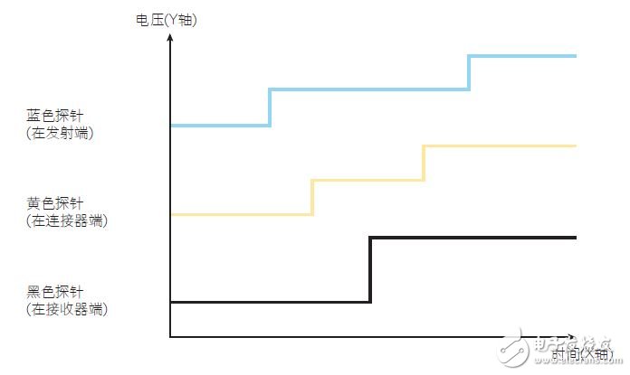
• The front end of the probe transmission line (the position at which the signal is output from the digital instrument transmitter) does not accurately display the signal received by the UUT. Since the signal transmits and reflects signals through the transmission line, it will "step" the digital signal on the oscilloscope.
• The middle of the probe transmission line (the junction box connects the digital instrument and the UUT) will also display a similar step digital signal, but not so much. The reason is the same: soon after seeing the signal pass, you will see the reflected wave returning to the digital instrument. Since the propagation time of the signal from the junction box to the UUT and back to the junction box is shorter than the round trip delay on the digital instrument, the step is less noticeable.
â— The best detection location is at the end of the transmission line and should be as close as possible to the receiver. This signal is closest to the digital wave actually received by the UUT.

Figure 4: Schematic diagram of Figure 3. Note that the black, yellow, and blue lines are possible probe points. Figure 5 shows the measured digital rising edge displayed on the oscilloscope.

Figure 5: The oscilloscope measures the digital rising edge at each probe point in the transmission line. The signal starts from the emitter (the first half of the blue probe) and propagates down the transmission line (yellow probe). The signal is reflected back to the generator at the receiver (black probe), doubling the amplitude of the signal. The reflected energy needs to be monitored at the yellow probe and the last blue probe, where the 50 Ω output impedance dissipates the reflected energy.
Note: Figure 5 above assumes a high impedance probe and the oscilloscope is terminated with a high impedance. Change the termination resistor to 50Ω and use a bare 50Ω cable to prevent signal reflection.
Measuring digital signal integrity in loopback testing
An important change in the device when performing loopback testing is that the path is twice as long as the previous example. This is because the signal is sent to both the UUT and the junction box and then terminated to the location where the signal was generated. It should be noted that the end of the transmission line is now in the digital instrument, we have to detect the position to accurately understand the digital signal on the receiver.
For NI digital instruments, this will require removing the housing of the VHDCI connector and using the probe to directly detect the wire. In many cases, this is not necessary for the application. If necessary, make sure that the measurements are taken at the correct location to properly display the actual digital signal received.

Figure 6: Schematic diagram of the loop test.
Measuring digital signal logic using digital instruments
There are applications that need to analyze the logic of a digital signal rather than the analog voltage level required for signal integrity testing. For these applications, using a digital instrument to probe the line or bus helps the user analyze the digital logic mode. An example of such an analysis is to connect a flying lead cable to both a high impedance digital input and another digital bus. Doing so may cause the cable to increase the load on the line and cause reflections. NI's solution to this problem is to use a 1 kΩ barrel attenuator to connect it to the front end of the flying cable, which reduces the loading effect of the probing cable on the system. For more information on this configuration, please visit the “Failure Collection†section of the Digital Fly Cable User Guide at ni.com.
Auto Transfer Switch,Automatic Transfer Switch,Emergency Transfer Switch,Automatic Changeover Switch
ZHEJIANG QIANNA ELECTRIC CO.,LTD , https://www.traner-elec.com