1 Introduction
The signal transmitter used on the ship is continuously operated, so a controller is needed to monitor the working state of the transmitter. It is common to use a single chip as the core of the controller, but because the 32-bit microprocessor has better precision and Reliability, low cost and low power consumption make it increasingly widely used in industrial control. Using the embedded 32-bit micro-processing ARMS3C44B0x as the core of the controller, the designed controller will have more comprehensive functions and better performance than the processor with the microcontroller as the core.
The main function of the transmitter controller is to monitor and monitor the working status of the multi-channel analog and digital data. The controller controls the transmitter and the controller is controlled by the host computer. It can be prepared at any time. It is good to receive data sent from the serial port and network port of the host computer. The relative relationship between them is as follows:

Figure 1 Controller system structure
The host computer sends data to the controller to control the controller. First, the host computer sends the machine number and sends the command word. The controller also uploads the data to the host computer to complete the communication response. It first analyzes whether the machine number and its own machine number. Consistently, if they are consistent, the command word is parsed again, and the uploaded data is sent according to the command word to complete the response; if not, no further data analysis is performed. Their communication methods are serial communication and Ethernet communication; the data transmission of controller and transmitter mainly has analog acquisition and switching input and output; in addition, the human interface module realizes the parameters in the working process of the transmitter. Real-time display and parameter modification and query. The data collected in real time is obtained by AD sampling. It should be noted that the S3c44B0 does not have a sample-and-hold circuit, so the switching frequency of the channel cannot exceed 100 Hz. A delay is required when the ADC is turned on. This time is used to filter the previous channel. And improve the efficiency of the program. The entire sampling process can be described as turning on the current channel and then filtering the last sampled channel (median value averaging filtering).
2. Switching machine description and software design
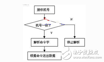
Figure 2 Flow communication flow chart
The development of the project must first complete the function of the switch machine, the function module of the man-machine interface, the programming and debugging of the communication module, first discuss the programming of the switch machine; the function of the user on the key of the controller is the function of each key that can be edited. Not fixed, can be modified by PC; when booting, it should output a series of actions from high to low in priority order, each action has editable priority (edited by PC), an action may cause after output The occurrence of other same priority level actions, this is the association of actions. It is necessary to detect the state of a higher priority action when the current priority action is turned on, and the fault needs to be handled when a fault occurs. Design the following data structure for the more complex requirements described above:
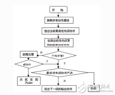
Figure 3 boot process
Typedef struct{
Char *pName; //action name
Char FuncTIonID; //Action (function) number
Char Priority; //Action priority
Short KeepTIme1; //waiting for the time required for the previous output action to stabilize
Short DelayTIme1; / / delay before the next action execution
Short DelayTIme2; //Time delay for repeated detection when detecting analog or switching
Short RepeatNum; / / number of fault re-detection
}OutputAction;
All functions are numbered sequentially, and the key is assigned to a key. The function is edited by modifying the value of OutputAction.FunctionID; each key has up to 16 functions, at least no function; All functions of each key are valid for round robin. Use a circular linked list to store the function number. The function corresponding to the position number of the header is always valid. Each function (action) can only belong to one key. When booting, the defined key function is sent to the controller by the serial port and programmed into the ROM of the fixed position; the editing of the action priority is realized by modifying the value of OutputAction.Priority in the structure; Read out the data, if the host computer does not perform key function editing, it will be in the default form. It should be pointed out that when the power is turned off, all output actions are closed in turn in the reverse order.
When booting, according to the content in the fixed position ROM or according to the default definition, the action attribute is obtained. 1 First, the action number with the highest priority is searched, and then these actions are sequentially sent according to different delays; 2 the priority is lowered by one level, and the detection is performed. Whether the status of all inputs and outputs higher than the current priority is normal. If it is normal, the current priority action is sent, and then the process of 2 is repeated. Otherwise, the fault processing procedure is entered. If the processing fault is successful, the process of repeating 2 is continued. Otherwise, Shut down and return to the boot failure message. The boot flow chart is shown in Figure 3.
One of the features in software design is the use of I/O ports to simulate the IIC bus to read key values. The general idea is to use two ports to simulate the IIC clock signal and the other to simulate the IIC data line. It should be noted that when configuring the I/O port, the port corresponding to the clock line is the output port and the data line port is undefined. The IIC data transmission protocol is simulated by setting and clearing the port delay. During the debugging process, it was found that this method can achieve key value acquisition and access to CPLD devices.
3. Human-machine interface module design
To monitor the working state of the transmitter, it must have a good man-machine interface. It is necessary to select the appropriate display device for the controller. In this project, a 7.8-inch 640×480 pixel STN color liquid crystal display (LCD) is used. Bit data scanning mode, the display effect is very good in practical applications, not only low cost and beautiful appearance, the interface of STN LCD screen and 44B0x is relatively simple, but it should be noted that the 18th pin (Vcom) is connected to the power supply through a varistor. Adjust the voltage on this pin to adjust the contrast of the LCD screen. The key in software design is menu design and button response and processing. Since there are many interfaces in this project and there are screens, it is advisable to design a unified processing algorithm. To this end, each interface is uniformly numbered WndID, and the button is used as the button. A message handles MessageFun(); each time you press a key, you call MessageFun(), find the interface you want to display and display it on the LCD. The method of flipping the LCD is to record the offset of the displayed content in the entire menu array each time. If the current line exceeds the offset, it needs to be turned over or not turned over. The design of the menu is as follows: a property is completely encapsulated by a structure, and its attributes include menu name, coordinates, parameter flags, and parameters.
Typedef struct{
UINT8T Menu_ID; / / menu number
UINT8T *Text; //Menu name
UINT16T xPos; //Menu x coordinate
UINT16T yPos; // menu y coordinate
UINT8T ParaFlag; //Parameter flag
UINT8T pData[7]; //parameter
}Menu;
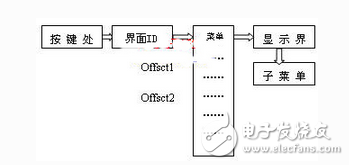
Figure 4 menu display
The structure is used to encapsulate the attributes of each menu and put them into an array. This has no limit on the number of menus and is easy to manage. The information of each menu is clear and the programming is not easy to make mistakes.
The core work of human-machine interface operation is interface switching, main menu and sub-menu operations. According to the button to determine the corresponding interface ID number, the method of switching the interface usually has two kinds of changes to the memory content and the base address of the change memory. To change the base address of the memory, it is necessary to define a large memory. The advantage of this is that the hardware resources are utilized. The LCD screen display has a high refresh rate and a fast interface switching. The disadvantage is that the system resources are greatly wasted; if the content in the video memory is changed, the software needs to be used to update the content in the memory. The advantage of this method is that it saves. System resources, but the complexity of the increased software design; the method used in this project to update the memory content found in the actual debugging can meet the requirements well. Regarding the operation of the main menu and submenu, a unified scheduling algorithm is designed. The idea is to determine the ID number of the main menu and the ID number of the sub menu according to the obtained key information, and use the focus to mark the ID number of the current menu. The ID number can determine that the corresponding main and submenu enter the corresponding function handler at the same time.
4. Ethernet communication module design
The hardware design is based on the RTL8019AS network control chip, which operates at 8 Mbps and has a transmission speed of 10 Mbps, following the IEEE 802.3 protocol. The internal 16KB SRAM integrates the functions of the MAC transceiver buffer and the physical layer. It is used to receive and transmit the physical transmission data of the Ethernet. When the RTL8019AS receives the network packet, the status of some control registers inside the RTL8019AS is changed. By setting the interrupt or query method to read the status of these registers to determine whether the data is received; when sending data, after the data is put into the RTL8019AS internal data buffer, the network data of the buffer is sent by controlling the internal registers. Go to the network. The chip has three modes of operation: jumper mode, plug and play mode, and jumper free mode. In the project, the network card chip RTL8019AS works in the jumper mode. The driving of the chip mainly includes the following steps: resetting, initializing, and transmitting and receiving data. The reset pin RSTDRV of RTL8019 is active high, the effective hold time should be greater than 800ns, and the chip operation is only after 100ms after switching from high to low. Before the chip is initialized, the space in the on-chip RAM, that is, the size of the receive and transmit buffers, needs to be pre-allocated, and all the set parameters are written together to the RTL8019 registers when initialization is completed.
5 Conclusion
There are many software and hardware difficulties in the process of project development and debugging, but the problem is solved continuously, such as serial port, LCD, AD sampling, debugging of Flash operation, and man-machine of controller. The programming of interactive functions needs to be debugged. After the Ethernet module is added to the project, the driver of the physical layer chip needs to be further debugged, and the TCP/IP protocol is added to the module, and the successful debugging case is completed to complete the debugging task of the system. At the same time, this article has the following innovations:
(1) Development and application of 32-bit micro-processing ARMS3C44B0x as the core of the controller, so that the controller has more comprehensive functions and better performance than the processor using the microcontroller as the core.
(2) In the design of the menu, a menu structure is completely encapsulated with a structure, and its attributes include menu name, coordinates, parameter flags, and parameters.
(3) Solved the problem that the network card chip makes the RTL8019AS work normally. Before initializing the chip, it is necessary to pre-allocate the space in the on-chip RAM, that is, the size of the receiving and sending buffers, and write all the setting parameters together when initializing. The register into the RTL8019 is initialized.
Vision SE is our specialist vision solution offering a wide range of classification services. Through advanced image processing, we realize professional-level visual technology, which is suitable for medical image processing, scientific research and other fields. We focus on performance optimization to make it an industrial-grade solution that is widely used in factory automation and high-demand application scenarios. At the same time, we pay attention to data security and privacy protection, ensuring that the highest standards are met when processing images and data. Vision SE's classified services exceed expectations, providing high-performance and professional-grade vision solutions to various industries.
vision services,vision sensor,vision sense,vision se,vision se review
Ningbo Autrends International Trade Co., Ltd. , https://www.visionsemr.com