The frequency synthesizer is the core device in the transmitting system and the receiving system. It adopts phase negative feedback frequency control technology, has good narrow-band carrier tracking performance and bandwidth modulation tracking performance, and provides local oscillator signal for phase up and down conversion, phase noise and The spurs have a good suppression effect, and the frequency source realized by the phase-locked frequency synthesis technology has been widely used in radar, communication, electronics and other fields.
This paper introduces the GPS signal source design as a reference, and introduces the typical application of ADI's frequency synthesizer ADF4360-4 in GPS signal source design.
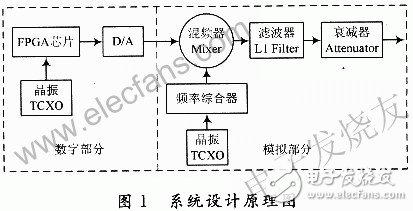
1 signal source system composition1.1 System Design
According to the literature, the structure characteristics of GPS signals are known. The purpose of designing GPS signal sources is to simulate the GPS signals transmitted by satellites, that is, baseband modulation of GPS signals and generate GPS RF signals with a frequency of 1 575.42 MHz. According to the literature, in the system. In the overall design, the super-heterodyne up-conversion idea is adopted. According to the system design features, the digital circuit and the analog circuit are divided into two parts. The system design is shown in Figure 1. The digital circuit part is designed with the idea of ​​software radio, and the GPS chip is used to complete the GPS signal. Baseband modulation and intermediate frequency modulation, output 8 b GPS digital intermediate frequency signal, converted to analog signal by D/A device and sent to analog circuit; analog circuit part is the core of the overall design, mainly for the design and implementation of RF circuit board The frequency synthesizer, the mixer and the like are used for mixing, filtering, power control, etc., and the GPS intermediate frequency signal is mixed and modulated to the radio frequency signal, and the up-conversion function is completed by using the radio frequency circuit.
1.2 Module design
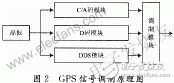
(1) Digital circuit: The digital circuit part is the baseband/IF module design. It adopts the software radio idea. According to the literature, the GPS chip is used to generate GPS navigation message (D code), C/A code and digital intermediate frequency carrier, and baseband modulation is performed on them. The spread spectrum modulation outputs the GPS digital intermediate frequency signal, wherein the GPS signal modulation principle is as shown in FIG. 2, and is mainly composed of a C/A code module, a D code module, a DDS module, and a modulation module. The C/A code module generates a C/A code sequence of the i-th satellite at a rate of 1.023 MHz, the C/A code has 1 023 chips, and the duration is 1 ms; the D code module generates the i-th rate of 50 Hz. Satellite navigation message (D code); DDS module generates digital carrier signal with rate of 12.5 MHz; modulation module performs spread spectrum modulation and BPSK modulation on C/A code, D code and carrier signal, and outputs 12.5 MHz GPS digital intermediate frequency signal .
(2) Analog circuit: According to the literature, the analog circuit part is the RF module design. The frequency synthesizer, mixer, filter and attenuator are used to design the RF circuit. The basic principle is the analog part shown in Figure 1. The GPS signal is moved from the intermediate frequency to the radio frequency, filtered by the filter, and the GPS RF signal is output after the power is adjusted by the adjustable attenuator to complete the up-conversion function.
2 frequency synthesizer ADF4360-42.1 Working principle and its performance
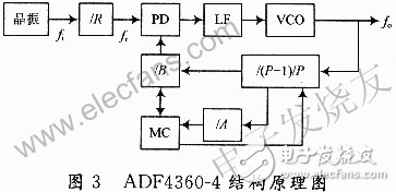
The main function of the frequency synthesizer is to provide local oscillator signals for system up-conversion. It is mostly used in transmitter and receiver system design, usually by digital phase detector (PD), loop filter (LF), voltage controlled oscillator ( VCO) and a programmable counter (R counter and N counter), etc., digital phase detector (PD) phase comparison of the output signals of the R calculator and the N counter to obtain an error voltage, through the loop filter (LF) The post-controlled voltage controlled oscillator (VCO) produces the desired frequency.
The frequency synthesizer ADF4360-4 is a high-performance phase-locked frequency synthesizer chip produced by Analog Devices. It is a dual-mode pre-frequency-divided single-loop frequency synthesizer that can effectively improve the frequency synthesizer without changing the frequency resolution. Output frequency; its main performance is, the output frequency range is 1450 ~ 1750 MHz, selectable two-way, the output signal frequency is 725 ~ 875 MHz when selecting the two-way frequency; the working voltage is 3 ~ 3.6V; the power of the output signal can be The control range is -13 to -4 dBm; the programmable dual-mode prescaler has a division ratio of 8/9, 16/17, 32/33; it can perform analog and digital lock detection; the VCO is integrated inside the chip. . The working principle of the ADF4360-4 is shown in Figure 3. P/(P+1) is a high-speed dual-mode prescaler with a frequency division modulus of P+1 and P. A is a 5-bit pulse swallow programmable counter. , B is a 13-bit main programmable counter, R is a 14-bit programmable reference divider, and MC is a mode control logic circuit. The device uses a programmable 5-bit A counter, a 13-bit B counter, and a dual-mode prescaler (P/P+1) to determine the main division ratio N (N=BP+A), a 14-bit programmable reference. The R frequency divider divides the external crystal oscillator to obtain the reference frequency fr=f0/R. Therefore, the design only needs to add a loop filter and select an appropriate reference value to obtain a stable frequency output. The output frequency is f0. =fi/R(A+BP), where fi is the input frequency and is provided by an external crystal.
2.2 Application Circuit Design
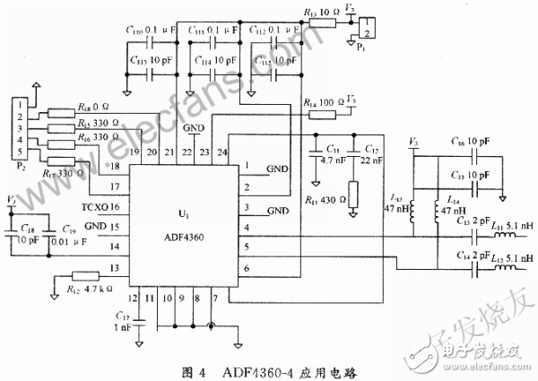
In the analog circuit RF module, the frequency synthesizer ADF4360-4 provides the local oscillator signal for the mixer. The application circuit is shown in Figure 4. The analog input of the frequency synthesizer is the external temperature-compensated crystal oscillator. The crystal oscillator passes the standard through a filter. The clock is sent to the 16-pin REFin of the ADF4360-4; the output pin of the frequency synthesizer is 4: RFoutA and 5-pin RFoutB, these two output differential high-frequency signals are fed into the mixer through the matching network and the resonant filter network. The differential input terminal; the 17th to 19th pins are respectively the CLK pin, the DATA pin, and the LE pin of the control data when the synthesizer is initialized, and are connected with the 20-pin MUXOUT for the test output to a 5-pin plug for the FPGA chip. Connection, as its input and output control interface; 12-pin Cc is the compensation pin, connected to a capacitor ground; 13-pin Rset is used to set the maximum current of the charge pump output, the current size is determined by the formula ICPmax=11.75/Rest, in this circuit Rest=4.7 kΩ; 14-pin CN is connected to Vvco decoupling with a capacitor; 6-pin VCO power supply, 21-pin digital power supply and 2-pin analog power supply are separately placed, respectively, decoupling capacitors are added; other analog ground and digital ground are directly grounded.
2.3 Initial design
The frequency synthesizer ADF4360-4 uses a high speed dual mode prescaler P, a 5-bit pulse swallow programmable counter A, a 13-bit main programmable counter B and a 14-bit programmable reference R divider to determine the main division ratio. Its output frequency is 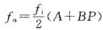
. In the analog circuit, the input crystal oscillator is fi=11.289 6 MHz, and the digital circuit output GPS signal frequency is 12.5 MHz. After calculation, the frequency synthesizer parameters A=5, B=34, P=8 can be set, so the frequency synthesizer output is The vibration signal frequency is .f0=1 563.609 8 MHz.
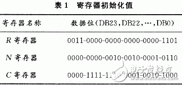
The frequency synthesizer ADF4360-4 has three 24-bit registers inside, R register, C register and N register. Since the register is used to temporarily store instructions and data, the data originally written to the register is lost after each power-down. Therefore, each time the power is turned on, the data must be written back to the register to obtain the desired local oscillator output. The register data write sequence in power-on is R register, C register and N register. The register data input program is written in VHDL language and controlled by FPGA chip. The initial setting values ​​of three 24-bit registers are shown in Table 1. The last two bits of each register DB1 and DB0 are used to determine the target register. For example, "01" stands for R register, "10" stands for N register, "00" stands for C register, and DB15~DB2 of R register is used to set 14 bit. Programmable reference divider R, N register DB20 ~ DB8 is used to set the 13-bit main programmable counter B, DB6 ~ DB2 is used to set the 5-bit pulse swallow programmable counter A, C register DB23 and DB22 used to determine the high speed Dual-mode prescaler P, for example, "OO" means P=8, and DB1 and DB12 of C register are used to set the output power. For example, "10" means that the frequency synthesizer output power is -7 dBm, which can be based on actual Need to adjust the output power
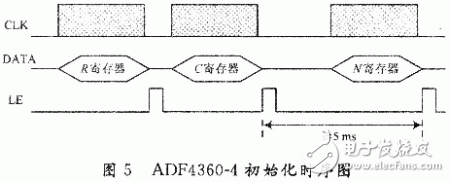
The three register data of ADF4360-4 is written by three bidirectional I/O ports of Analog Devices' FPGA chip PlC6Q240C8. The connection principle is shown in Figure 4. The three bidirectional I/O ports of the FPGA chip are respectively Connect the LE pin, DATA pin, and CLK pin of the ADF4360-4, where CLK is the serial clock input, DATA is the serial data input, and LE is the load enable. The ADF4360-4 initialization timing is shown in Figure 5. First, the data in the 24-bit shift register is sequentially written from the MSB (most significant bit) on the rising edge of each CLK by the DATA pin, and the input 24 b data is loaded to the target at one time according to the rising edge signal of the LE pin. The register is then initialized to the next destination register, where the assignment interval between the C and N registers should be greater than 5 ms.
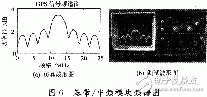
The core of the digital circuit module is the baseband/IF module. It uses the FPGA chip EP1C6Q240C8 from Analog Devices. The chip uses 130 nm technology and has 5 980 logic units. It is tested under the Quart-usII8.O platform. The test result is occupied by GPS signal modulation. 337 logic units, using ModelSim simulation platform, write TestBench test file, export GPS signal data with 1 ms duration under ModelSim platform, perform power spectrum analysis on Matlab, simulation waveform is shown in Figure 6(a), center frequency is 12.5 MHm sends the GPS IF signal output from the baseband/IF module to the Aetna spectrum analyzer AT5011 for spectrum analysis. The spectrum waveform is shown in Figure 6(b). The signal center frequency is 12.5 MHz. The IF signal energy is mainly concentrated on the main lobe. The simulation results are consistent with the measured results.
When the RF module of the analog circuit is designed for PCB circuit, the problem to be considered is noise interference. Noise interference is an important factor affecting the performance of the RF circuit. In the PCB layout, the interference between the digital circuit and the analog circuit should be considered. High-power device Interference with low-power devices, noise interference from power supply, wiring and grounding of high-frequency lines. The verification of the RF module is to observe whether the GPS IF signal is upconverted to a signal of 1 575.42 MHz. In the test, the GPS RF signal output by the RF module is attenuated by 60 dB and sent to the spectrum analyzer. The spectrum display signal is a single frequency signal. The center frequency is 1 575.4 MHz and the test meets the system setting requirements.
4 ConclusionBy analyzing the working principle, performance characteristics and application circuit design of frequency synthesizer ADF4360-4, combined with GPS signal source design, the overall design scheme of GPS signal source with FPGA chip and frequency synthesizer as the core is proposed. The two parts of the analog circuit were designed and implemented, and the experimental test was given. The results show that the baseband/IF module with FPGA as the core realizes BPSK modulation of GPS signal, spread spectrum modulation, and outputs GPS IF signal of 12.5 MHz. The RF module with frequency synthesizer ADF4360-4 as the core completes the up-conversion function. The GPS IF signal is modulated onto the RF 1 575.4 MHz, and the test meets the system design requirements.
All in one pc is a new trend for desktop type computer nowadays. What you can see at this store is Custom All In One PC. There are 19 inch all in one pc, 21.5 All In One PC, All In One PC 23.8 Inch and 27 inch all in one pc, which are the main sizes at the market. How to choose the most suitable one for special application? According to clients` feedback, 19.1 inch entry level, 21.5 inch middle and low level, 23.8 or 27 inch higher level-All In One PC I7. Some clients may worry the heat-releasing since equipped releasing fan into the back of monitor, see no releasing fences on back cover. However, totally no need worry that point, cause special back cover material and releasing holes can meet the demand of heat releasing.
You can see All In One Business Computer, All In One Gaming PC, and All In One Desktop Touch Screen series at this shop.
Any other unique design or parameters, just feel free to contact us so that can get right and value information quickly.
Believe will try our best to support you!
All In One PC,All In One Pc I7,Custom All In One Pc,All In One Pc 23.8 Inch,21.5 All In One Pc
Henan Shuyi Electronics Co., Ltd. , https://www.shuyielectronics.com