In order to adapt to the diversity of embedded device peripherals, this paper designs a complete set of drive control modules by taking a special matrix keyboard as an example. The hardware circuit design adopts the method of expanding three SN74HC 164 chips, which saves the use of GPIO pins and greatly improves the utilization efficiency. At the same time, based on this, the characteristics and working mechanism of the input subsystem in the Linux kernel are introduced, and the process of transmitting the complete input events from the kernel space to the user space process is presented. The experimental results show that the designed driver module has good real-time and accuracy.
With the continuous development of microprocessor technology and the popularity of digital products, the research and development of embedded systems has gradually become a hot spot. Linux has become the mainstream of embedded operating systems with its advantages of open source, stability and tailorability. Among the many embedded systems, the keyboard has become the most widely used input device. However, the functional difference of embedded devices determines that it is not feasible to provide a universal keyboard. It is often necessary to design a special keyboard according to the actual function of the system and implement the corresponding driver.
The S3C6410 is a high-performance 32-bit RISC microprocessor from Samsung. It integrates a variety of powerful hardware accelerators for video and image processing, making it the mainstream product in the embedded processor field. Taking a 24-key matrix keyboard based on S3C6410 microprocessor as an example, this paper presents the overall process of developing device drivers in embedded systems, and studies and analyzes the underlying transfer mechanism of input events under Linux system.
1 interface circuit design
The common way to expand the keyboard on the embedded device is to scan the GPIO port of the CPU. Obviously, this method will occupy too much GPIO resources and increase the GPIO port resources when the number of keyboard keys is large. The burden of a tight embedded processor.
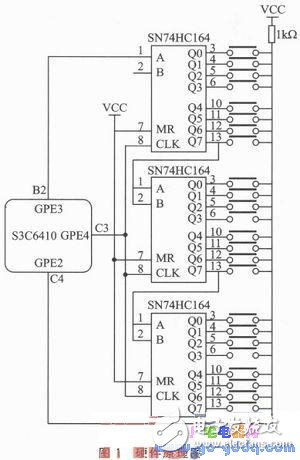
The hardware design of this system achieves the goal of saving GPIO resources by adding three SN74HC164 chips. The SN74HC164 is an 8-bit serial input, parallel output shift register that is internally connected by eight D flip-flops. Whenever the clock signal changes from low to high, the two inputs pass the current input signal to the parallel output and implement a shift operation. The system hardware schematic is shown in Figure 1.

After the three SN74HC164 chips are connected in series, connect their CLK pins to the GPE4 port of the S3C6410 development board. The A and B input pins of the first SN74HC164 chip are connected to the GPE3 port of the development board, and the two GPIO ports are configured in output mode. The GPE2 port is connected to the pull-up end of the keyboard button, and the system switches between the interrupt mode and the input mode during operation to achieve the purpose of triggering the interrupt and scanning the keyboard. In this way, we use three SN74HC164 shift registers, occupying only three GPIO ports, and providing input signals to the 24 keys of the scan keyboard, which saves cost and avoids waste of GPIO resources.
2 How the scan works
Extending the hardware circuit brings some trouble to the implementation of the keyboard driver. The driver must first drive the SN74HC164 before it can control the circuit. The output pin of this circuit is connected to the GPE2 port of the S3C6410, and this port is configured as an interrupt source, which is directly read as high when no key is pressed. When the keyboard scans, the SN74HC164 chip first sets the 24 keys of the keyboard to a low level. When any key is pressed, the GPE2 port will jump from a high level to a low level, thereby triggering an interrupt.
The GPE2 port is placed in the input state during interrupt processing. Then according to the input/output characteristics of the SN74HC164 chip, 24 high-level signals are sent to the three SN74HC164 chips in series, so that the keys of the keyboard are all high. At the next 24 clock pulses, the SN74HC164 chip is fed a 0 and 23 1 so that 0 appears only once at the input of each key and is scanned at the GPE2 port. When the pressed key is in the 0 input state, its line will read a low level, and it can be determined which key on the keyboard has been pressed.
3 drive module structure
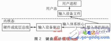
A new addition to the input subsystem in the Linux 2.6 release provides the driver writer with a complete input event -- a model passed from the underlying device to the user process. Based on the input subsystem architecture, this paper designs a more perfect special keyboard driver module. The structure of the keyboard driver module is shown in Figure 2.

In the device kernel model of the input subsystem, the most important data structure is struct input_dev, which is the body of the driver. Each strucTInput_dev represents an input device. The structure contains both input event types, response button types, keyboard code tables, and coordinate fields, as well as fields such as device open, close, and callback functions, which can completely record and Identify the function and behavior of the entire device. Before registering input_dev with the kernel, you need to initialize the input_dev structure and apply for a keyboard interrupt to the kernel.
5.1 Column Speaker,Column Array Speakers,Column Speakers,Column Speaker System
GUANGZHOU SOWANGNY ELECTRONIC CO.,LTD , https://www.jerry-power.com